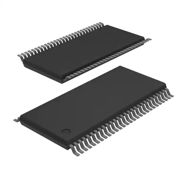
This 12-bit to 24-bit multiplexed D-type latch is designed for 1.65-V to 3.6-V VCC operation.
The SN74ALVCH16260DL is used in applications in which two separate data paths must be multiplexed onto, or demultiplexed from, a single data path. Typical applications include multiplexing and/or demultiplexing address and data information in microprocessor or bus-interface applications. This device also is useful in memory-interleaving applications.
Three 12-bit I/O ports (A1-A12, 1B1-1B12, and 2B1-2B12) are available for address and/or data transfer. The output-enable (OE1B\, OE2B\, and OEA\) inputs control the bus transceiver functions. The OE1B\ and OE2B\ control signals also allow bank control in the A-to-B direction.
Address and/or data information can be stored using the internal storage latches. The latch-enable (LE1B, LE2B, LEA1B, and LEA2B) inputs are used to control data storage. When the latch-enable input is high, the latch is transparent. When the latch-enable input goes low, the data present at the inputs is latched and remains latched until the latch-enable input is returned high.
To ensure the high-impedance state during power up or power down, OE\ should be tied to VCC through a pullup resistor; the minimum value of the resistor is determined by the current-sinking capability of the driver.
Active bus-hold circuitry is provided to hold unused or floating data inputs at a valid logic level.
The SN74ALVCH16260DL is characterized for operation from –40°C to 85°C.
Feature
- Member of the Texas Instruments Widebus Family
- EPIC (Enhanced-Performance Implanted CMOS) Submicron Process
- ESD Protection Exceeds 2000 V Per MIL-STD-883, Method 3015; Exceeds 200 V Using Machine Model (C = 200 pF, R = 0)
- Latch-Up Performance Exceeds 250 mA Per JESD 17
- Bus Hold on Data Inputs Eliminates the Need for External Pullup/Pulldown Resistors
- Package Options Include Plastic Shrink Small-Outline (DL) and Thin Shrink Small-Outline (DGG) Packages


