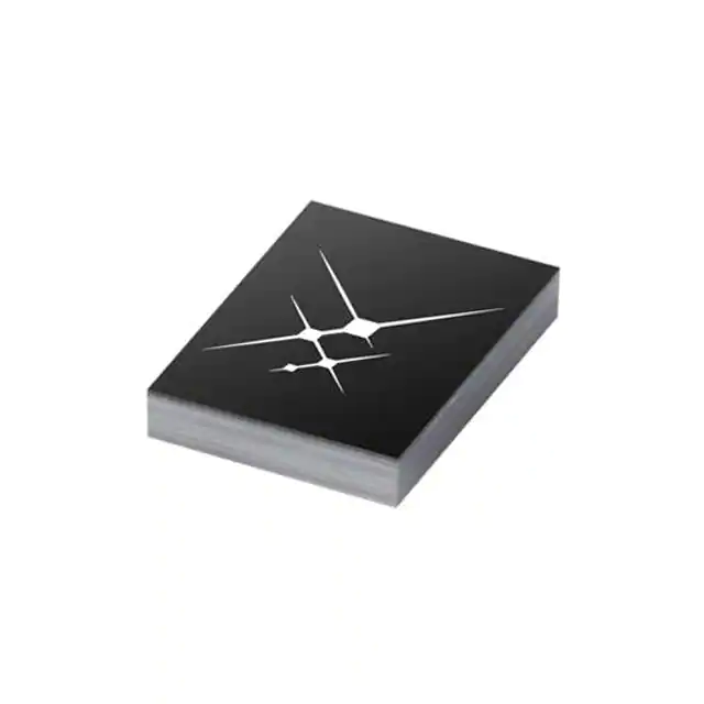
The output voltage of the device is controlled by an analog signal from the baseband processor. The SKY87000-13-001 can support up to 2 A of total load current with step-down and bypass regulators. The 2 MHz switching frequency is optimized for a typical 2.2 μH inductor and reduced output capacitance.
To further improve system performance, an 85 mΩ bypass linear regulator is included that allows the PA to be powered directly from the battery. The bypass regulator output voltage is offset from the step-down regulator, which improves extreme load transient and dynamic output transition performance.
The SKY87000-13-001 is available in a 9-bump Wafer Level Chip Scale Package (WLCSP) with 0.5 mm pin pitch.
Feature
- Input voltage range: 2.7 to 5.5 V
- Dynamic output voltage: 0.4 V to 4.25 V
- 0.16 V to 1.7 V reference input range
- 2.5 times the reference input voltage to regulator output gain
- Internally compensated current/mode architecture:
- 2 MHz switching frequency
- 2.2 μH chip inductor
- Two 4.7 μF output capacitors
- Wide duty cycle range (100% duty cycle operation)
- Integrated 85 mΩ (typical) bypass regulator
- Less than 10 μs response for 1 V output step
- Up to 2 A typical output current
- Small 9-bump WLCSP package (MSL1, 260 °C per JEDEC J-STD-020) package
Applications
- Smartphones
- 4G LTE


