Component qualification in accordance with JEDEC and industry standards to ensure reliable operation over an extended temperature range. This includes, but is not limited to, Highly Accelerated Stress Test (HAST) or biased 85/85, temperature cycle, autoclave or unbiased HAST, electromigration, bond intermetallic life, and mold compound life. Such qualification testing should not be viewed as justifying use of this component beyond specified performance and environmental limits.
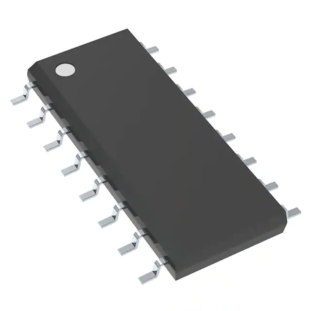
DescriptionThis parallel-in or serial-in, serial-out register features gated clock (CLK, CLK INH) inputs and an overriding clear (CLR)\ input. The parallel-in or serial-in modes are established by the shift/load (SH/LD\) input. When high, SH/LD\ enables the serial (SER) data input and couples the eight flip-flops for serial shifting with each clock (CLK) pulse. When low, the parallel (broadside) data inputs are enabled, and synchronous loading occurs on the next clock pulse. During parallel loading, serial data flow is inhibited. Clocking is accomplished on the low-to-high-level edge of CLK through a 2-input positive-NOR gate, permitting one input to be used as a clock-enable or clock-inhibit function. Holding either CLK or CLK INH high inhibits clocking; holding either low enables the other clock input. This allows the system clock to be free running, and the register can be stopped on command with the other clock input. CLK INH should be changed to the high level only when CLK is high. CLR\ overrides all other inputs, including CLK, and resets all flip-flops to zero.
Feature
- Controlled Baseline
- One Assembly/Test Site, One Fabrication Site
- Enhanced Diminishing Manufacturing Sources (DMS) Support
- Enhanced Product-Change Notification
- Qualification Pedigree
- Wide Operating Voltage Range of 2 V to 6 V
- Outputs Can Drive Up To 10 LSTTL Loads
- Low Power Consumption, 80-μA Max ICC
- Typical tpd = 13 ns
- ±4-mA Output Drive at 5 V
- Low Input Current of 1 μA Max
- Synchronous Load
- Direct Overriding Clear
- Parallel-to-Serial Conversion
Component qualification in accordance with JEDEC and industry standards to ensure reliable operation over an extended temperature range. This includes, but is not limited to, Highly Accelerated Stress Test (HAST) or biased 85/85, temperature cycle, autoclave or unbiased HAST, electromigration, bond intermetallic life, and mold compound life. Such qualification testing should not be viewed as justifying use of this component beyond specified performance and environmental limits.
DescriptionThis parallel-in or serial-in, serial-out register features gated clock (CLK, CLK INH) inputs and an overriding clear (CLR)\ input. The parallel-in or serial-in modes are established by the shift/load (SH/LD\) input. When high, SH/LD\ enables the serial (SER) data input and couples the eight flip-flops for serial shifting with each clock (CLK) pulse. When low, the parallel (broadside) data inputs are enabled, and synchronous loading occurs on the next clock pulse. During parallel loading, serial data flow is inhibited. Clocking is accomplished on the low-to-high-level edge of CLK through a 2-input positive-NOR gate, permitting one input to be used as a clock-enable or clock-inhibit function. Holding either CLK or CLK INH high inhibits clocking; holding either low enables the other clock input. This allows the system clock to be free running, and the register can be stopped on command with the other clock input. CLK INH should be changed to the high level only when CLK is high. CLR\ overrides all other inputs, including CLK, and resets all flip-flops to zero.


