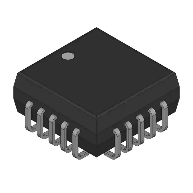
These 8-bit universal shift/storage registers feature multiplexed I/O ports to achieve full 8-bit data handling in a single 20-pin package. Two function-select (S0, S1) inputs and two output-enable (OE1\, OE2\) inputs can be used to choose the modes of operation listed in the function table.
Synchronous parallel loading is accomplished by taking both S0 and S1 high. This places the 3-state outputs in the high-impedance state and permits data applied on the I/O ports to be clocked into the register. Reading out of the register can be accomplished while the outputs are enabled in any mode. Clearing occurs asynchronously when the clear (CLR\) input is low. Taking either OE1\ or OE2\ high disables the outputs, but has no effect on clearing, shifting, or storing data.
The SN54ALS299 is characterized for operation over the full military temperature range of -55°C to 125°C. The SN74ALS299DW is characterized for operation from 0°C to 70°C.
Feature
- Multiplexed I/O Ports Provide Improved Bit Density
- Four Modes of Operation:
- Hold (Store)
- Shift Right
- Shift Left
- Load Data
- Operate With Outputs Enabled or at High Impedance
- 3-State Outputs Drive Bus Lines Directly
- Can Be Cascaded for n-Bit Word Lengths
- Direct Overriding Clear
- Applications:
- Stacked or Push-Down Registers
- Buffer Storage
- Accumulator Registers
- Package Options Include Plastic Small-Outline (DW) Packages, Ceramic Chip Carriers (FK), and Standard Plastic (N) and Ceramic (J) 300-mil DIPs


