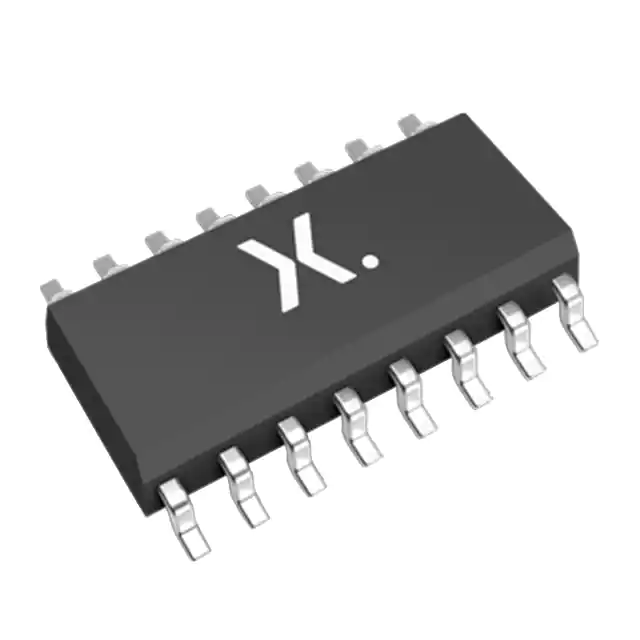
The HEF4014BT is a 8-bit static Shift Register with eight synchronous parallel inputs (D0 to D7), a synchronous serial data input (DS), a synchronous parallel enable input (PE), a low-to-high edge-triggered clock input (CP) and buffered parallel outputs from the last three stages (Q5 to Q7). Operation is synchronous and the device is edge-triggered on the low-to-high transition of CP. Each register stage is of a D-type master-slave flip-flop type. When PE is high, data is loaded into the register from D0 to D7 on the low-to-high transition of CP. When PE is low, data is shifted to the first position from DS and all the data in the register is shifted one position to the right on the low-to-high transition of CP. The clock input's Schmitt trigger action makes it highly tolerant of slower clock rise and fall times. It operates over a recommended VDD power supply range of 3 to 15V referenced to VSS (usually ground). Unused inputs must be connected to VDD, VSS or another input.
Feature
- Tolerant of slow clock rise and fall times
- Fully static operation
- Standardized symmetrical output characteristics
- Complies with JEDEC standard JESD 13-B

