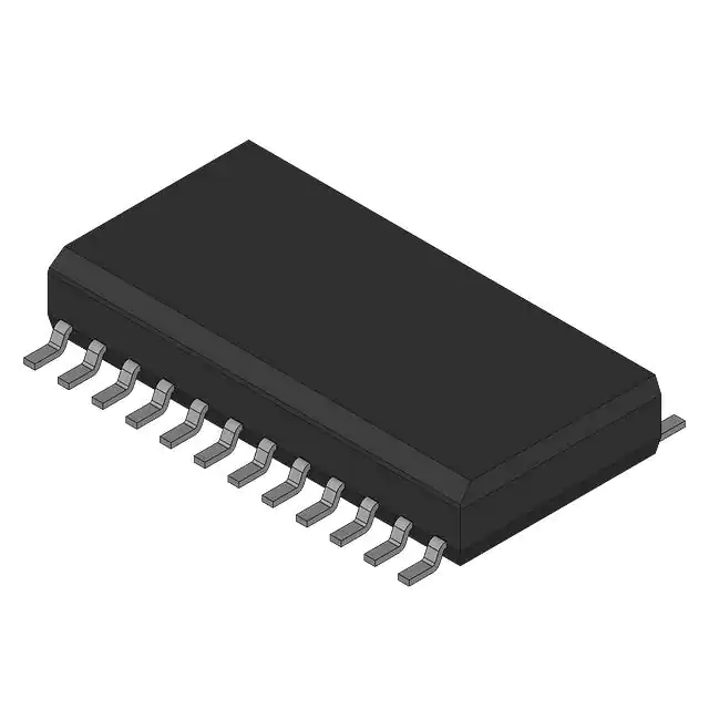
The CD74FCT843AM is a 9-bit, bus-interface, D-type latch with 3-state outputs, designed specifically for driving highly capacitive or relatively low-impedance loads. It is particularly suitable for implementing buffer registers, I/O ports, bidirectional bus drivers, and working registers.
The device uses a small-geometry BiCMOS technology. The output stage is a combination of bipolar and CMOS transistors that limits the output high level to two diode drops below VCC. This resultant lowering of output swing (0 V to 3.7 V) reduces power-bus ringing [a source of electromagnetic interference (EMI)] and minimizes VCC bounce and ground bounce and their effects during simultaneous output switching. The output configuration also enhances switching speed and is capable of sinking 48 mA.
The CD74FCT843AM outputs are transparent to the inputs when the latch-enable (LE) input is high. The latches are transparent D-type latches. When LE goes low, the data is latched. The output-enable (OE\) input controls the 3-state outputs. When OE\ is high, the outputs are in the high-impedance state. The latch operation is independent of the state of the output enable. This device, having preset (PRE\) and clear (CLR\), are ideal for parity-bus interfacing. When PRE\ is low, the outputs are high if OE\ is low. PRE\ overrides CLR\. When CLR\ is low, the outputs are low if OE\ is low. When CLR\ is high, data can be entered into the latch. The device provides noninverted outputs.
OE\ does not affect the internal operations of the latch. Previously stored data can be retained or new data can be entered while the outputs are in the high-impedance state.
The CD74FCT843AM is characterized for operation from 0°C to 70°C.
Feature
- BiCMOS Technology With Low Quiescent Power
- Buffered Inputs
- Noninverted Outputs
- Input/Output Isolation From VCC
- Controlled Output Edge Rates
- 48-mA Output Sink Current
- Output Voltage Swing Limited to 3.7 V
- SCR Latch-Up-Resistant BiCMOS Process and Circuit Design
- Packaged in Plastic Small-Outline Package
The CD74FCT843A is a 9-bit, bus-interface, D-type latch with 3-state outputs, designed specifically for driving highly capacitive or relatively low-impedance loads. It is particularly suitable for implementing buffer registers, I/O ports, bidirectional bus drivers, and working registers.
The device uses a small-geometry BiCMOS technology. The output stage is a combination of bipolar and CMOS transistors that limits the output high level to two diode drops below VCC. This resultant lowering of output swing (0 V to 3.7 V) reduces power-bus ringing [a source of electromagnetic interference (EMI)] and minimizes VCC bounce and ground bounce and their effects during simultaneous output switching. The output configuration also enhances switching speed and is capable of sinking 48 mA.
The CD74FCT843A outputs are transparent to the inputs when the latch-enable (LE) input is high. The latches are transparent D-type latches. When LE goes low, the data is latched. The output-enable (OE\) input controls the 3-state outputs. When OE\ is high, the outputs are in the high-impedance state. The latch operation is independent of the state of the output enable. This device, having preset (PRE\) and clear (CLR\), are ideal for parity-bus interfacing. When PRE\ is low, the outputs are high if OE\ is low. PRE\ overrides CLR\. When CLR\ is low, the outputs are low if OE\ is low. When CLR\ is high, data can be entered into the latch. The device provides noninverted outputs.
OE\ does not affect the internal operations of the latch. Previously stored data can be retained or new data can be entered while the outputs are in the high-impedance state.
The CD74FCT843A is characterized for operation from 0°C to 70°C.


