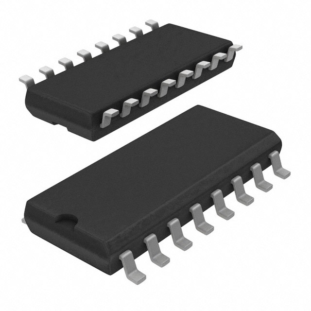
The MC14049BFELG Hex Inverter/Buffer and MC14050B Noninverting Hex Buffer are constructed with MOS P-Channel and N-Channel enhancement mode devices in a single monolithic structure. These complementary MOS devices find primary use where low power dissipation and/or high noise immunity is desired. These devices provide logic level conversion using only one supply voltage, VDD. The input-signal high level (VIH) can exceed the VDD supply voltage for logic level conversions. Two TTL/DTL loads can be driven when the devices are used as a CMOS-to-TTL/DTL converter (VDD = 5.0 V, VOL <= 0.4 V, IOL >=3.2 mA). Note that pins 13 and 16 are not connected internally on these devices; consequently connections to these terminals will not affect circuit operation.
Feature
- High Source and Sink Currents
- High-to-Low Level Converter
- Supply Voltage Range = 3.0 V to 18 V
- VIN can exceed VDD
- Meets JEDEC B Specifications
- Improved ESD Protection On All Inputs
- Pb-Free Packages are Available*
(Picture: Pinout)
