Features:
·3-state parallel outputs for connection to common bus Separate serial outputs synchronous to both positive and negative clock edges for cascading aMedium speed operation-5 MHz at 10 V(typ.)Standardized, symmetrical output characteristics
·100% tested for quiescent current at 20V aMaximum input current of 1 uA at 18 V over full package temperature range;100 nA at 18 V and 25c
■Noise margin (full package temperature range):1 Vat VDp=5V2Vat VDp=10V.5Vat Vop=15V·5-V,10-V, and 15-V parametric ratings aMeets all requirements of JEDEC Tentative Standard No.13B,"Standard Specifications for Description of 'B' Series CMOS Devices"
Applications:
Serial-to-parallel data conversion
Remote control holding register aDual-rank shift,hold,and bus applications
CD4094B is an 8-stage serial shift register having a storage latch associatedwith each stage for strobing data from the serial input to parallel buffered 3-state out-puts. The parallel outputs may be connected directly to common bus lines. Data is shifted on positive clock transitions. The data in each shift register stage is transferred to the storage register when the STROBE input is high. Data in the storage register appears at the outputs whenever the OUTPUT-ENABLE signal is high.
Two serial outputs are available for cascading a number of CD4094B devices. Data is available at the Os serial output terminal on positive clock edges to allow for high-speed operation in cascaded systems in which the clock rise time is fast. The same serial infor.mation, available at the Q's terminal on the next negative clock edge, provides a means for cascading CD4094B devices when the clock rise time is slow.
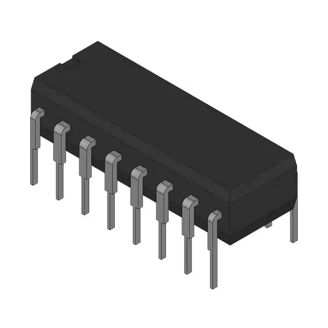
The CD4094B types are supplied in 16-lead hermetic dual-in-line ceramic packages (F3A suffix),16-lead dual-in-line plastic packages(E suffix),16-lead small-outline packages(NSR suffix), and 16-lead thinshrink small-outline packages (PW and PWR suffixes).
Feature
- Low quiescent current - 10 nA/pkg (typ.) at VDD = 5 V
- Clock frequency 12 MHz (typ.) at VDD = 10 V
- Schmitt trigger clock inputs allow operation with very slow clock rise and fall times
- Capable of driving two low-power TTL loads, one low-power Schottky TTL load, or two HTL loads
- Three-state outputs
- 100% tested for quiescent current at 20 V
- Standardized, symmetrical output characteristics
- 5-V, 10-V and 15-V parametric ratings
- Meets all requirements of JEDEC Tentative Standard No. 13B, Standard Specifications for Description of 'B' Series CMOS Devices
- Applications: Time-delay circuits Scratch-pad memories General-purpose serial shift-register applications
CD4517B dual 64-stage static shift register consists of two independent registers each having a clock, data, and write enable input and outputs accessible at taps following the 16th, 32nd, 48th, and 64th stages. These taps also serve as input points allowing data to be inputted at the 17th, 33rd, and 49th stages when the write enable input is a logic 1 and the clock goes through a low-to-high transition. The truth table indicates how the clock and write enable inputs control the operation of the CD4517B. Inputs at the intermediate taps allow entry of 64 bits into the register with 16 clock pulses. The 3-state outputs permit connection of this device to an external bus.
The CD4517B is supplied in 16-lead hermetic dual-in-line ceramic packages (D and F suffixes), 16-lead dual-in-line plastic packages (E suffix), and in chip form (H suffix).
(Picture: Pinout)


