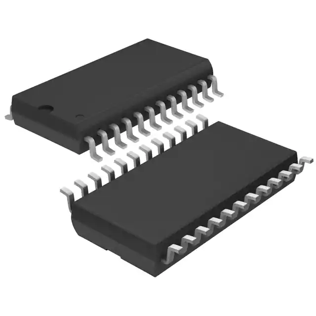
The device consists of an 8-bit shift register,8 latches, and control logic to perform the polarity select and blanking of theoutputs. Data is shifted through the shift register on the low to high transition of the clock.A data output buffer is provided forcascading devices. Operation of the shift register is not affected by the LE, BL, POL, or the HI-Z control inputs. Transfer of data from the shift register to the latch occurs when the LE is high. The data in the latch is stored when LE is low.A high-Z, HI-Z, pin is provided to set all the outputs in a high-Z state.
Alloutputs have short circuit protection that detects if the outputs have reached the required output state. If output does not track the required state, then the SHORT pin will be low. This output will pulse low during the output transistion period under normal operation; see SC Timing Diagram for details.
All outputs will have a break-before-make circuitry to reduce cross-over current during output state changes.
The POL,B, LE, and HI-Z inputs have an internal pull up resistor.
Features
- HVCMOS,technology
- Operating output voltage of 250V
- Low power level shifting from 5V to 250V
- Shift register speed 8MHz@Voo=5V
- 8 latch data outputs
- Output polarity and blanking
- CMOS compatible inputs
- Output short circuit detect
- Output high-Z contro
Applications
- Piezoelectric transducer driver
- Weaving applications
- Braille
- Printers
- MEMs
- Displays
Feature
- HVCMOS® technology
- Operating output voltage of 250V
- Low power level shifting from 5.0 to 250V
- Shift register speed 8.0MHz @ VDD = 5.0V
- 8 latch data outputs
- Output polarity and blanking
- Output short circuit detect
- Output high-Z control
- CMOS compatible inputs
(Picture:Pinout / Diagram)


