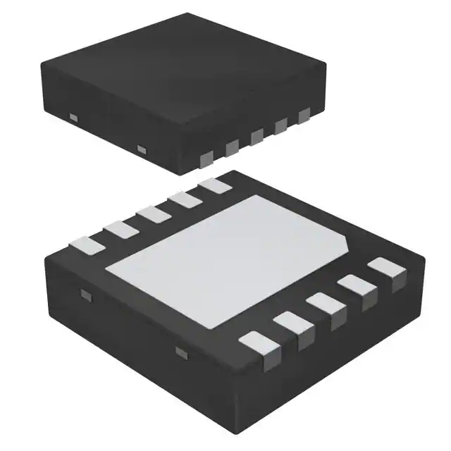
The TPS51217DSCT is a small-sized single buck controller withadaptive on-time D-CAP? mode. The device is suitable for low outputvoltage, high current, PC system power rail and similar point-of-load(POL) power supply in digital consumer products. A small package withminimal pin-count saves space on the PCB, while a dedicated EN pin andpre-set frequency minimize design effort required for new designs. Theskip-mode at light load condition, strong gate drivers and low-side FET RDS(on)current sensing supports low-loss and high efficiency, over a broadload range. The TRAN pin provides freedom of masking overvoltageprotection, undervoltage protection and power-good signal during thetransition period of dynamic output voltage change for modern GPU powersupply applications. The conversion input voltage which is the high-sideFET drain voltage ranges from 3 V to 28 V and the output voltage rangesfrom 0.6 V to 2.6 V. The device requires an external 5-V supply. TheTPS51217DSCT is available in a 10-pin SON package specified from –40°C to85°C.
Feature
- Wide Input Voltage Range: 3 V to 28 V
- Output Voltage Range: 0.6 V to 2.6 V
- Wide Output Load Range: 0 to 20A+
- Built-in 0.5% 0.6 V Reference
- D-CAP Mode with 100-ns Load Step Response
- Adaptive On Time Control Architecture with Fixed 340kHz Operation
- Dynamic Output Voltage Change Capability
- 4700 ppm/°C RDS(on) Current Sensing
- Internal 0.9-ms Voltage Servo Softstart
- Pre-Charged Start-up Capability
- Built-in Output Discharge
- Power Good Output
- Integrated Boost Switch
- Built-in OVP/UVP/OCP
- Thermal Shutdown (Non-latch)
- SON-10 (DSC) Package
The TPS51217 is a small-sized single buck controller withadaptive on-time D-CAP? mode. The device is suitable for low outputvoltage, high current, PC system power rail and similar point-of-load(POL) power supply in digital consumer products. A small package withminimal pin-count saves space on the PCB, while a dedicated EN pin andpre-set frequency minimize design effort required for new designs. Theskip-mode at light load condition, strong gate drivers and low-side FET RDS(on)current sensing supports low-loss and high efficiency, over a broadload range. The TRAN pin provides freedom of masking overvoltageprotection, undervoltage protection and power-good signal during thetransition period of dynamic output voltage change for modern GPU powersupply applications. The conversion input voltage which is the high-sideFET drain voltage ranges from 3 V to 28 V and the output voltage rangesfrom 0.6 V to 2.6 V. The device requires an external 5-V supply. TheTPS51217 is available in a 10-pin SON package specified from –40°C to85°C.


