The input voltage range of 2.85 V to 15 V supports a wide variety of applications. The integrated main switch enables the generation of an adjustable negative output voltage down to 39 V below the input voltage.
The ADP5074ACPZ-R7 operates at a pin selected 1.2 MHz/2.4 MHz switching frequency. The ADP5074ACPZ-R7 can synchronize with an external oscillator from 1.0 MHz to 2.6 MHz to ease noise filtering in sensitive applications. The regulator implements programmable slew rate control circuitry for the MOSFET driver stage to reduce electromagnetic interference (EMI).
The ADP5074ACPZ-R7 includes a fixed internal or resistor programmable soft start timer to prevent inrush current at power-up. During shutdown, the regulator completely disconnects the load from the input supply to provide a true shutdown. A power good pin is available to indicate the output is stable.
Other key safety features in the ADP5074ACPZ-R7 include overcurrent protection (OCP), overvoltage protection (OVP), thermal shutdown (TSD), and input undervoltage lockout (UVLO).
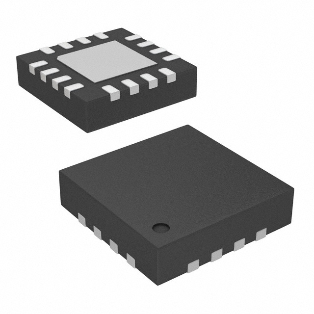
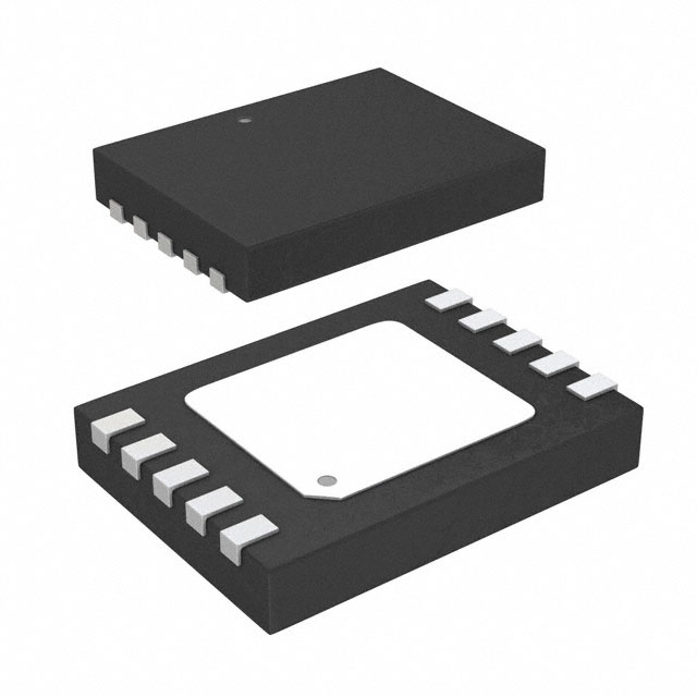
The ADP5074ACPZ-R7 is available in a 16-lead LFCSP and is rated for a −40°C to +125°C operating junction temperature range.
Feature
- Wide input voltage range: 2.85 V to 15 V
- Adjustable negative output to VIN − 39 V
- Integrated 2.4 A main switch
- 1.2 MHz/2.4 MHz switching frequency with optional external frequency synchronization from 1.0 MHz to 2.6 MHz
- Resistor programmable soft start timer
- Slew rate control for lower system noise
- Precision enable control
- Power-good output
- UVLO, OCP, OVP, and TSD protection
- 3 mm × 3 mm, 16-lead LFCSP
- −40°C to +125°C junction temperature
- Supported by the ADIsimPower tool set
Applications
- Bipolar amplifiers, ADCs, digital-to-analog converters (DACs), and multiplexers
- High speed converters
- Radio frequency (RF) power amplifier (PA) bias
- Optical modules
(Picture: Pinout)

