This is the product guarantees long time support in Industrial market. is a synchronous buck switching regulator with built-in power MOSFETs. It is capable of an output current 2.5A. It has a high oscillation frequency of 1MHz while using small inductance value. is a current mode control DC/DC converter and features high-speed transient response. Phase compensation can also be set easily.
Input Voltage Range: to 36V Output Voltage Range: to VIN�0.7V Output Current: 2.5A (Max) Switching Frequency: 1MHz (Typ) High-Side MOSFET ON-Resistance: 170m (Typ) Low-Side MOSFET ON-Resistance: 140m (Typ) Standby Current: 0A (Typ) W (Typ) x D (Typ) x H (Max) x 1.00mm
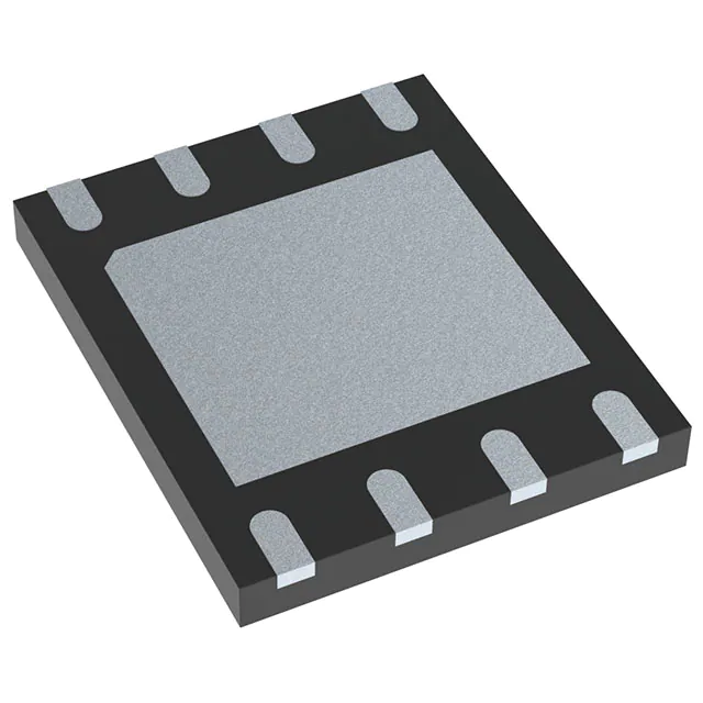
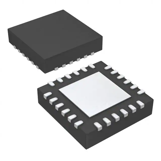
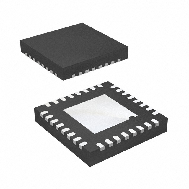
FeaturesLong Time Support Product for Industrial Applications. Synchronous single DC/DC converter. Over-Current Protection. Short Circuit Protection. Thermal Shutdown Protection. Undervoltage Lockout Protection. Soft Start. HTSOP-J8 package (Exposed Pad).
ApplicationsIndustrial Equipment. Power supply for FA's industrial device using 24V bass. Consumer applications such as home appliance. Distribution type power supply system for 12V, and 24V. HTSOP-J8
Product structureSilicon monolithic integrated circuit. www.rohm.com � 2013 ROHM Co., Ltd. All rights reserved. TSZ2211114001
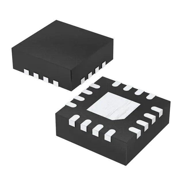
This product has no designed protection against radioactive rays.(TOP VIEW) BOOT VIN EN AGND 1 2 E-Pad 3 4 Figure 2. Pin assignment 6 5 COMP 7 SW PGND
Pin No 1 Pin Name BOOT Description Connect a bootstrap capacitor of 0.1�F between this terminal and SW terminal. The voltage of this capacitor is the gate drive voltage of the high-side MOSFET. Power supply terminal for the switching regulator and control circuit. Connecting a 10�F ceramic capacitor is recommended. Turning this terminal signal low-level (0.8V or lower) forces the device to enter the shut down mode. Turning this terminal signal high-level (2.5V or higher) enables the device. This terminal must be terminated. Ground terminal for the control circuit. Inverting input node for the gm error amplifier. See page 22 on how to calculate the resistance of the output voltage setting. Input terminal for the gm error amplifier output and the output switch current comparator. Connect a frequency phase compensation component to this terminal. See page 23 on how to calculate the resistance and capacitance for phase compensation. Ground terminal for the output stage of the switching regulator. Switch node. This terminal is connected to the source of the high-side MOSFET and drain of the low-side MOSFET. Connect a bootstrap capacitor of 0.1�F between this terminal and BOOT terminal. In addition, connect an inductor considering the direct current superimposition characteristic. Exposed pad. Connecting this to the internal PCB ground plane using multiple vias provides excellent heat dissipation characteristics.
www.rohm.co � 2013 ROHM Co., Ltd. All rights reserved. TSZ2211115001Feature
- Long Life Cycle Product for IndustrialApplications.
- Synchronous single DC/DC converter.
- Over-Current Protection.
- Short Circuit Protection.
- Thermal Shutdown Protection.
- Undervoltage Lockout Protection.
- Soft Start.