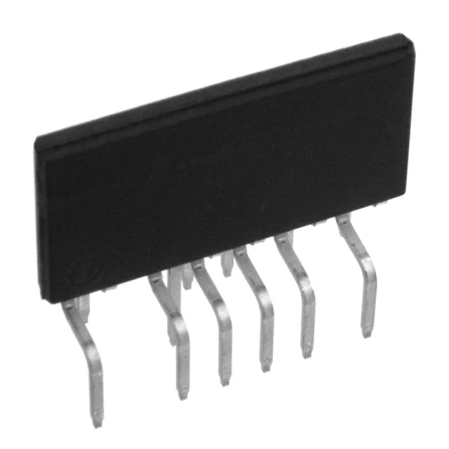
Combined Two-Switch Forward and Flyback Power Supply Controllers with Integrated High-Voltage MOSFETs
Selectable 132 kHz main switching frequency for lower cost and smaller magnetics Increased main peak power vs. HiperTFS-1 Self-biased high-side driver eliminates high-side bias winding and diode Package lead form and pinout modified for easier insertion and PC-board layout Tighter UV(ON) standby threshold tolerance Improved standby no-load performance
586 W peak output power in a highly compact package >90% efficiency at full load Simple clip mounting to heat sink without need for insulation pad Halogen free and RoHS compliant
Key Benefits Single IC solution for two-switch forward main (66 kHz/132 kHz) and flyback (132 kHz) standby High integration allows smaller form factor and higher power density designs, with reduced component count Incorporates control, gate drivers, and three power MOSFETs Level shift technology eliminates need for pulse transformer Protection features include: UV, OV, OTP, OVP, standby OPC, SCP, and ILIMIT Transformer reset control, prevents saturation under all conditions Main duty cycle operation above 50% for reduced rms currents and lower output diode voltage rating Less than 10% variation in standby overload power over input voltage range
Typical Applications PC (80 PLUS� Bronze and 80 PLUS Silver) Printer LCD TV Video game consoles High-power adapters Industrial and appliance Output Power Table
Table 1. Output Power Table. Notes: 1. Maximum practical continuous power in an open frame design with adequate heat sinking to maintain a heat sink temperature 95 �C (see Key Applications Considerations for more information) measured at specified ambient temperature. 2 Peak load less than 10 seconds and average power less than maximum continuous load. 3. Package: eSIP-16F. (Note: Direct attach to heat sink, does not require insulation SIL pad).
Schematic of Two-Switch Forward and Flyback Converter. November 2013This Product is Covered by Patents and/or Pending Patent Applications.
Description................................................................................................................................................................... 3 Product Highlights....................................................................................................................................................... 3 Pin Functional Description.......................................................................................................................................... 5 Pin Configuration....................................................................................................................................................... 5 Functional Block Diagram......................................................................................................................................6-7 Functional Description................................................................................................................................................ 8 Design, Assembly and Layout Considerations...................................................................................................... 14 Layout Considerations............................................................................................................................................... 17 Transformer Secondary and Output Diodes............................................................................................................ 21 Main Converter Typical Waveforms.......................................................................................................................... 22 Quick Design Checklist.............................................................................................................................................. 23 Design Example.......................................................................................................................................................... 25 Absolute Maximum Ratings...................................................................................................................................... 27 Parameter Table...................................................................................................................................................... 27 Package Details......................................................................................................................................................... 34 Part Ordering Information......................................................................................................................................... 40 Part Marking Information......................................................................................................................................... 41
Description The HiperTFS-2 device family members incorporate both a high-power two-switch-forward converter and a mid-power flyback (standby) converter into a single, low-profile eSIPTM power package. The single chip solution provides the controllers for the two-switch-forward and flyback converters, high- and low-side drivers, all three of the high-voltage power MOSFETs, and eliminates the converter's need for costly external pulse transformers. The device is ideal for high power applications that require both a main power converter (two-switch forward) 586 W peak, and standby converter (flyback) W. HiperTFS-2 includes Power Integrations' standard set of comprehensive protection features, such as integrated softstart, fault and overload protection, and hysteretic thermal shutdown. HiperTFS-2 utilizes advanced power packaging technology that simplifies the complexity of two-switch forward layout, mounting and thermal management, while providing very high power capabilities in a single compact package. The devices operate over a wide input voltage range, and can be used following a power-factor correction stage such as HiperPFS. Two-switch-forward power converters are often selected for applications demanding cost-effective converters that have high efficiency, fast transient response, and high rejection to line voltage variation. The two-switch-forward controller incorporated into HiperTFS-2 devices improves on the classic topology by allowing operation considerably above 50% duty cycle. This improvement reduces RMS current conduction losses, minimizes the size and cost of the bulk capacitor, and minimizes output diode voltage ratings. The advanced design also includes transformer flux reset control (saturation protection) and charge-recovery switching of the high-side MOSFET, which reduces switching losses. This combination of innovations yields an extremely efficient power supply with smaller MOSFETs, fewer passives and discrete components, and a lower-cost smaller transformer. HiperTFS-2's flyback standby controller and MOSFET solution is based on the highly popular TinySwitchTM technology used in billions of power converter ICs due to its simplicity of operation, light load efficiency, and rugged, reliable, performance. This flyback converter can provide W of output power and the built-in overload power compensation reduces component design margin.
Accurate hysteretic thermal shutdown (OTP) Accurate selectable cycle-by-cycle current limit (main and standby) Line compensated standby MOSFET current limit for standby over power compensation (OPC) Fully integrated soft-start to minimize start-up stress Simple fast AC reset Reduced EMI Synchronized 66/132 kHz forward and 132 kHz flyback converters Frequency jitter Eliminates to 30 discrete components for higher reliability and lower cost Output short-circuit protection (SCP) with auto-restart
Asymmetrical Two-Switch Forward Reduces Losses Allows >50% duty cycle operation Reduces primary-side RMS currents and conduction losses Minimizes the size and cost of the bulk capacitor Allows reduced capacitance or longer hold-up time Allows lower voltage output diodes for higher efficiency Transformer reset control Prevents transformer saturation under all conditions Extends duty cycle to satisfy AC cycle drop out ride through Duty cycle soft-start Satisfies 20 ms start-up with large capacitance at output Self-biased high-side driver eliminates high-side bias winding (66 kHz) Remote-on/off function Voltage-mode controller with current limit 20 W Flyback with Selectable Power Limit TinySwitch-III based converter Selectable power limit W, 20 W) Built-in overload power compensation (OPC) Flat overload power vs. input voltage Reduces component stress during overload conditions Reduces required design margin for transformer and output diode Output overvoltage (OVP) protection with fast AC reset Latching, non-latching, or auto-restart Auto-restart Advanced Package for High Power Applications 586 W peak output power capability in a highly compact package Simple clip mounting to heat sink Can be directly connected to heat sink without insulation pad Provides lower thermal resistance than a TO-220 Heat slug connected to ground potential for low EMI Two row lead form for easy insertion into PC-board Single power package for two power converters reduces assembly costs and layout size
Protected Two-Switch Forward and Flyback Combination Solution Incorporates three high-voltage power MOSFETs, main and standby controllers, and gate drivers Level shift technology eliminates need for pulse transformer Programmable line undervoltage (UV) detection prevents turn-off glitches Programmable line overvoltage (OV) detection; latching and non-latching


