Widebus is a trademark of Texas Instruments Incorporated.
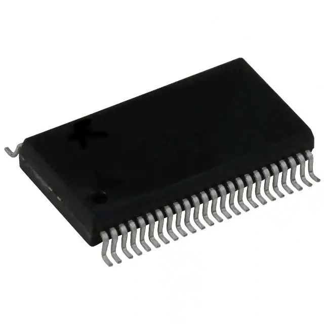
DescriptionThis 9-bit to 18-bit D-type latch is designed for 3.15-V to 3.45-V VCC operation. The D inputs accept HSTL levels and the Q outputs provide LVTTL levels.
The SN74HSTL16918DGGR is particularly suitable for driving an address bus to two banks of memory. Each bank of nine outputs is controlled with its own latch-enable (LE\) input.
Each of the nine D inputs is tied to the inputs of two D-type latches that provide true data (Q) at the outputs. While LE\ is low, the Q outputs of the corresponding nine latches follow the D inputs. When LE\ is taken high, the Q outputs are latched at the levels set up at the D inputs.
The SN74HSTL16918DGGR is characterized for operation from 0°C to 70°C.
Output level before the indicated steady-state input conditions were established
Feature
- Member of the Texas Instruments WidebusTM Family
- Inputs Meet JEDEC HSTL Std JESD 8-6 and Outputs Meet Level III Specifications
- ESD Protection Exceeds 2000 V Per MIL-STD-883, Method 3015; Exceeds 200 V Using Machine Model (C = 200 pF, R = 0)
- Latch-Up Performance Exceeds 250 mA Per JESD 17
- Packaged in Plastic Thin Shrink Small-Outline Package
Widebus is a trademark of Texas Instruments Incorporated.
DescriptionThis 9-bit to 18-bit D-type latch is designed for 3.15-V to 3.45-V VCC operation. The D inputs accept HSTL levels and the Q outputs provide LVTTL levels.
The SN74HSTL16918 is particularly suitable for driving an address bus to two banks of memory. Each bank of nine outputs is controlled with its own latch-enable (LE\) input.
Each of the nine D inputs is tied to the inputs of two D-type latches that provide true data (Q) at the outputs. While LE\ is low, the Q outputs of the corresponding nine latches follow the D inputs. When LE\ is taken high, the Q outputs are latched at the levels set up at the D inputs.
The SN74HSTL16918 is characterized for operation from 0°C to 70°C.
Output level before the indicated steady-state input conditions were established


