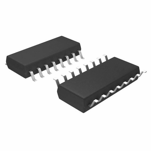
CD4031BNSRG4 is a static shift register that contains 64 D-type, master-slave flip-flop stages and one stage which is a D-type master flip-flop only (referred to as a 1/2 stage).
The logic level present at the DATA input is transferred into the first stage and shifted one stage at each positive-going clock transition.Maximum clock frequencies up to 12 Megahertz (typical) can be obtained.Because fully static operation is allowed, information can be permanently stored with the clock line in either the low or high state.The CD4031BNSRG4 has a MODE CONTROL input that, when in the high state, allows operation in the recirculating mode.The MODE CONTROL input can also be used to select between two separate data sources.Register packages can be cascaded and the clock lines driven directly for high-speed operation.Alternatively, a delayed clock output (CLD) is provided that enables cascading register packages while allowing reduced clock drive fan-out and transition-time requirements.A third cascading option makes use of the Q' output from the 1/2 stage, which is available on the next negative-going transition of the clock after the Q output occurs.This delayed output, like the delayed clock CLD, is used with clocks having slow rise and fall times.
The CD4031BNSRG4 types are supplied in 16-lead hermetic dual-in-line ceramic packages (F3A suffix), 16-lead dual-in-line plastic packages (E suffix), 16-lead small-outline packages (NSR suffix), and 16-lead thin shrink small-outline packages (PW and PWR suffixes).
Feature
- Fully static operation: DC to 12 MHz typ. @ VDD - VSS = 15 V
- Standard TTL drive capability on Q output
- Recirculation capability
- Three cascading modes:
- Direct clocking for high-speed operation
- Delayed clocking for reduced clock drive requirements
- Additional 1/2 stage for slow clocks
- 100% tested for quiescent current at 20 V
- Maximum input current of 1 μA at 18 V over full package-temperature range; 100nA at 18 V and 25°C
- Noise margin (over full package-temperature range):
1 V at VDD = 5 V
2 V at VDD = 10 V
2.5 V at VDD = 15 V - 5-V, 10-V, and 15-V parametric ratings
- Meets all requirements of JEDEC Tentative Standard No. 13A, "Standard Specifications for Description of 'B' Series CMOS Devices"
- Applications:
- Serial shift register
- Time delay circuits


