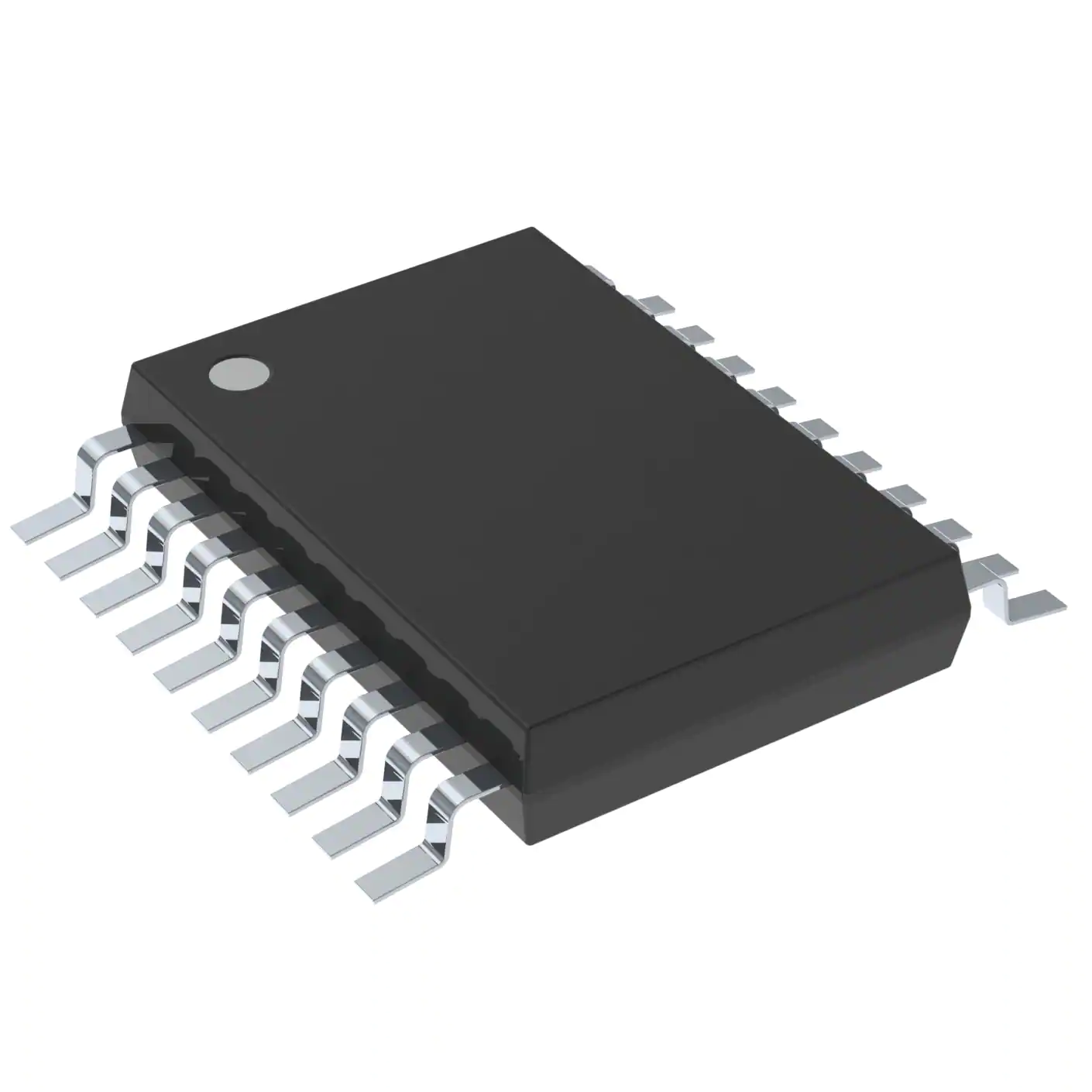
These 8-bit latches are designed specifically for storing the contents of the input data bus and providing the capability of reading back the stored data onto the input data bus. The Q outputs are designed with bus-driving capability.
The edge-triggered flip-flops enter the data on the low-to-high transition of the clock (CLK) input when the enable () input is low. Data can be read back onto the data inputs by taking the read () input low, in addition to having low. When EN\ is high, both the read-back and write modes are disabled. Transitions on should only be made with CLK high to prevent false clocking.
The polarity of the Q outputs can be controlled by the polarity (T/C\) input. When T/C\ is high, Q is the same as is stored in the flip-flops. When T/C\ is low, the output data is inverted. The Q outputs can be placed in the high-impedance state by taking the output-enable () input high.does not affect the internal operation of the register. Old data can be retained or new data can be entered while the outputs are off.
A low level at the clear () input resets the internal registers low. The clear function is asynchronous and overrides all other register functions.
The -1 version of the SN74ALS996DWR is identical to the standard version, except that the recommended maximum IOL for the -1 version is increased to 48 mA. There is no -1 version of the SN54ALS996.
The SN54ALS996 is characterized for operation over the full military temperature range of -55°C to 125°C. The SN74ALS996DWR is characterized for operation from 0°C to 70°C.
Feature
- 3-State I/O-Type Read-Back Inputs
- Bus-Structured Pinout
- T/C\ Determines True or Complementary Data at Q Outputs
- Package Options Include Plastic Small-Outline (DW) Packages,Ceramic Chip Carriers (FK), and Standard Plastic (NT) and Ceramic(JT) 300-mil DIPs
These 8-bit latches are designed specifically for storing the contents of the input data bus and providing the capability of reading back the stored data onto the input data bus. The Q outputs are designed with bus-driving capability.
The edge-triggered flip-flops enter the data on the low-to-high transition of the clock (CLK) input when the enable () input is low. Data can be read back onto the data inputs by taking the read () input low, in addition to having low. When EN\ is high, both the read-back and write modes are disabled. Transitions on should only be made with CLK high to prevent false clocking.
The polarity of the Q outputs can be controlled by the polarity (T/C\) input. When T/C\ is high, Q is the same as is stored in the flip-flops. When T/C\ is low, the output data is inverted. The Q outputs can be placed in the high-impedance state by taking the output-enable () input high.does not affect the internal operation of the register. Old data can be retained or new data can be entered while the outputs are off.
A low level at the clear () input resets the internal registers low. The clear function is asynchronous and overrides all other register functions.
The -1 version of the SN74ALS996 is identical to the standard version, except that the recommended maximum IOL for the -1 version is increased to 48 mA. There is no -1 version of the SN54ALS996.
The SN54ALS996 is characterized for operation over the full military temperature range of -55°C to 125°C. The SN74ALS996 is characterized for operation from 0°C to 70°C.


