Description
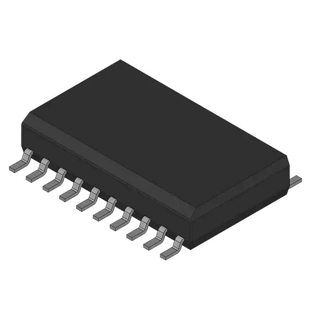
These Schottky TTL eight-bit universal registers feature multiplexed inputs/outputs to achieve full eight-bit data handling in a single 20-pin package. Two function-select inputs and two output-control inputs can be used to choose the modes of operation listed in the function table.
Synchronous parallel loading is accomplished by taking both function-select lines, S0 and S1, high. This places the three-state outputs in a high-impedance state, which permits data that is applied on the input/output lines to be clocked into the register. Reading out of the register can be accomplished while the outputs are enabled in any mode. A direct overriding input is provided to clear the register whether the outputs are enabled or off.
Feature
- Multiplexed Inputs/Outputs Provide Improved Bit Density
- Four Modes of Operations:
- Hold (Store)
- Shift Left
- Shift Right
- Load Data
- Operates with Outputs Enabled or at High Z
- 3-State Outputs Drive Bus Lines Directly
- Can Be Cascaded for N-Bit Word Lengths
- SN54LS323 and SN74LS323 Are Similar But Have Synchronous Clear
- Applications:
- Stacked or Push-Down Registers Buffer Storage, and Accumulator Registers
Description
These Schottky TTL eight-bit universal registers feature multiplexed inputs/outputs to achieve full eight-bit data handling in a single 20-pin package. Two function-select inputs and two output-control inputs can be used to choose the modes of operation listed in the function table.
Synchronous parallel loading is accomplished by taking both function-select lines, S0 and S1, high. This places the three-state outputs in a high-impedance state, which permits data that is applied on the input/output lines to be clocked into the register. Reading out of the register can be accomplished while the outputs are enabled in any mode. A direct overriding input is provided to clear the register whether the outputs are enabled or off.


