INTEGRATED CIRCUITS DATA SHEET FAMILY SPECIFICATIONS HCMOS family characteristics March 1988 File under Integrated Circuits, IC06 Philips Semiconductors HCMOS family characteristics GENERAL These family specifications cover the common electrical ratings and characteristics of the entire HCMOS 74HC/HCT/HCU family, unless otherwise specified in the individual device data sheet. INTRODUCTION The 74HC/HCT/HCU high-speed Si-gate CMOS logic family combines the low power advantages of the HE4000B family with the high speed and drive capability of the low power Schottky TTL (LSTTL). The family will have the same pin-out as the 74 series and provide the same circuit functions. In these families are included several HE4000B family circuits which do not have TTL counterparts, and some special circuits. The basic family of buffered devices, designated as XX74HCXXXXX, will operate at CMOS input logic levels for high noise immunity, negligible typical quiescent supply and input current. It is operated from a power supply of 2 to 6 V. FAMILY SPECIFICATIONS A subset of the family, designated as XX74HCTXXXXX, with the same features and functions as the “HC-types”, will operate at standard TTL power supply voltage (5 V ± 10%) and logic input levels (0.8 to 2.0 V) for use as pin-to-pin compatible CMOS replacements to reduce power consumption without loss of speed. These types are also suitable for converted switching from TTL to CMOS. Another subset, the XX74HCUXXXXX, consists of single-stage unbuffered CMOS compatible devices for application in RC or crystal controlled oscillators and other types of feedback circuits which operate in the linear mode. HANDLING MOS DEVICES Inputs and outputs are protected against electrostatic effects in a wide variety of device-handling situations. However, to be totally safe, it is desirable to take handling precautions into account (see also “HANDLING PRECAUTIONS”). RECOMMENDED OPERATING CONDITIONS FOR 74HC/HCT 74HC2G32DC SYMBOL PARAMETER min. typ. VCC VI VO Tamb Tamb tr, tf DC supply voltage DC input voltage range DC output voltage range 2.0 0 0 5.0 max. 6.0 VCC VCC +85 +125 1000 6.0 500 400 Note 1. For analog switches, e.g. “4016”, “4051 series”, “4351 series”, “4066” and “4067”, the specified maximum operating supply voltage is 10 V. 6.0 500 ns min. typ. max. 4.5 0 0 −40 −40 5.0 5.5 VCC VCC +85 +125 V V V °C °C see DC and AC CHAR. per device VCC = 2.0 V VCC = 4.5 V VCC = 6.0 V 74HCT UNIT CONDITIONS operating ambient temperature range −40 operating ambient temperature range −40 input rise and fall times except for Schmitt-trigger inputs March 1988 2 Philips Semiconductors HCMOS family characteristics RECOMMENDED OPERATING CONDITIONS FOR 74HCU FAMILY SPECIFICATIONS 74HCU SYMBOL VCC VI VO Tamb Tamb PARAMETER min. typ. max. DC supply voltage DC input voltage range DC output voltage range operating ambient temperature range operating ambient temperature range 2.0 0 0 −40 −40 5.0 6.0 […]

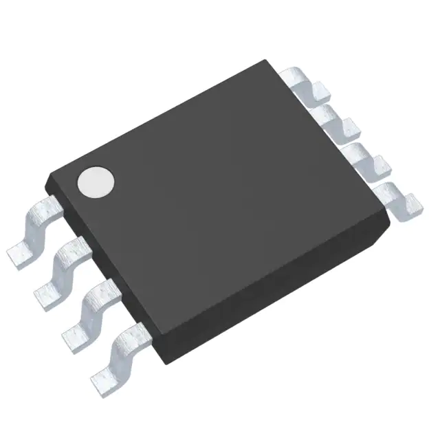
74HC2G32DC-Q100H
- 描述:逻辑类型: OR门 电线数量: two 输入数量: two 电源电压: 2V~6V 供应商设备包装: 8-VSSOP 安装类别: 表面安装
- 品牌: 安世半导体 (Nexperia)
- 交期:5-7 工作日
渠道:
- 自营
- 得捷
- 贸泽
起订量: 3000
| 数量 | 单价 | 合计 |
|---|---|---|
| 3000+ | 1.99817 | 5994.51300 |
- 库存: 0
- 单价: ¥1.99817
-
数量:
- +
- 总计: ¥5,994.51
在线询价
温馨提示: 请填写以下信息,以便客户代表及时与您沟通联系。
规格参数
- 部件状态 可供货
- 输入数量 two
- 特点 -
- 安装类别 表面安装
- 最大静态电流 1.A.
- 逻辑类型 OR门
- 工作温度 -40摄氏度~125摄氏度
- 电源电压 2V~6V
- 输出高电流, 输出低电流 5.2毫安, 5.2毫安
- 电线数量 two
- 低逻辑电平 0.5V~1.8V
- 高逻辑电平 1.5伏~4.2伏
- 最大传播延迟 @ 电压(V), 最大负载电容(CL) 13ns @ 6V, 50皮法
- 包装/外壳 8-VFSOP (0.091", 2.30毫米 Width)
- 制造厂商 安世半导体 (Nexperia)
- 供应商设备包装 8-VSSOP
74HC2G32DC-Q100H 产品详情
74HC2G32DC-Q100H所属分类:逻辑门/反相器,74HC2G32DC-Q100H 由 安世半导体 (Nexperia) 设计生产,可通过久芯网进行购买。74HC2G32DC-Q100H价格参考¥1.998171,你可以下载 74HC2G32DC-Q100H中文资料、PDF数据手册、Datasheet数据手册功能说明书,可查询74HC2G32DC-Q100H规格参数、现货库存、封装信息等信息!
安世半导体 (Nexperia)

Nexperia是大批量生产基本半导体的领先专家,这些半导体是世界上每一种电子设计所需的元件。该公司广泛的产品组合包括二极管、双极晶体管、ESD保护装置、MOSFET、GaN FET以及模拟和逻辑IC。...


