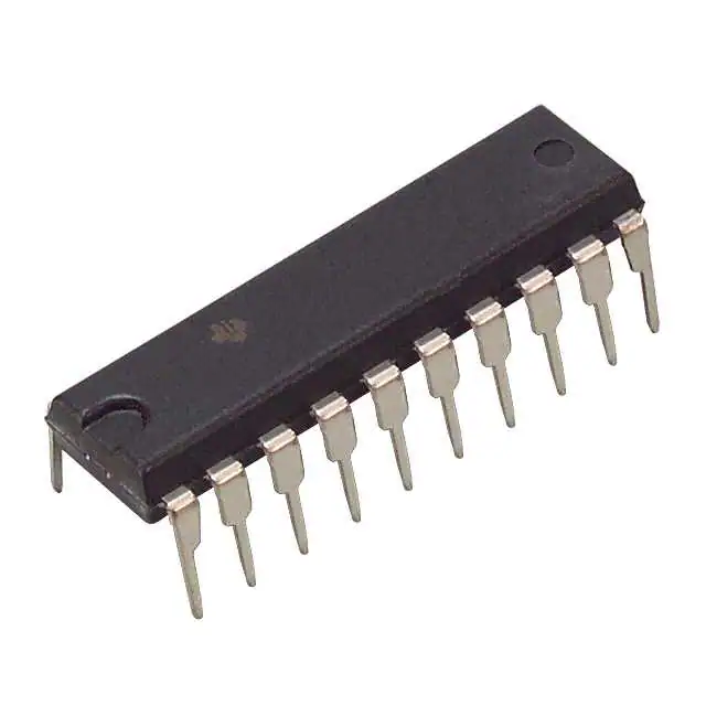
The CD74HCT356E consists of data selectors/multiplexers that select one of eight sources. The data select bits (S0, S1, and S2) are stored in transparent latches that are enabled by a low latch enable input (LE\).
The data is stored in edge-triggered flip-flops that are triggered by a low-to-high clock transition.
In both types the 3-state outputs are controlled by three output-enable inputs (OE1\, OE2\, and OE3).
Feature
- Edge-Triggered Data Flip-Flops
- Transparent Select Latches
- Buffered Inputs
- 3-State Complementary Outputs
- Bus Line Driving Capability
- Typical Propagation Delay: VCC= 5V, CL = 15pF, TA = 25°C
- Clock to Output = 22ns
- Fanout (Over Temperature Range)
- Standard Outputs. . . . . . . . . . . . . . . 10 LSTTL Loads
- Bus Driver Outputs . . . . . . . . . . . . . 15 LSTTL Loads
- Wide Operating Temperature Range . . . -55°C to 125°C
- Balanced Propagation Delay and Transition Times
- Significant Power Reduction Compared to LSTTL Logic ICs
- 4.5V to 5.5V Operation
- Direct LSTTL Input Logic Compatibility, VIL = 0.8V (Max), VIH = 2V (Min)
- CMOS Input Compatibility, Il 1μA at VOL, VOH


