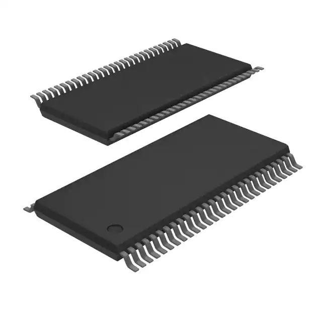
The SN74CB3T16211DGGR is a high-speed TTL-compatible FET bus switch with low ON-state resistance (ron), allowing for minimal propagation delay. The device fully supports mixed-mode signal operation on all data I/O ports by providing voltage translation that tracks VCC. The SN74CB3T16211DGGR supports systems using 5-V TTL, 3.3-V LVTTL, and 2.5-V CMOS switching standards, as well as user-defined switching levels.
The I/O port of this device has a pullup current source that maintains the output voltage at VCC when the device is ON, and the input is greater than or equal to VCC– 1. Because of the pullup current source, the output voltage level may be less than VCC when the operating frequency is low and the I/O port is connected to a pulldown resistor. In order to maintain the output voltage at VCC, a pullup resistor must be connected to VCC instead of a pulldown resistor to ground.
The SN74CB3T16211DGGR is organized as two 12-bit bus switches with separate output-enable (1OE should be tied to VCC through a pullup resistor; the minimum value of the resistor is determined by the current-sinking capability of the driver.
Feature
- Member of the Texas Instruments Widebus Family
- Output Voltage Translation Tracks VCC
- Supports Mixed-Mode Signal Operation on All Data I/O Ports
- 5-V Input Down to 3.3-V Output Level Shift With 3.3-V VCC
- 5-V/3.3-V Input Down to 2.5-V Output Level Shift With 2.5-V VCC
- 5-V Tolerant I/Os With Device Powered Up or Powered Down
- Bidirectional Data Flow With Near-Zero Propagation Delay
- Low ON-State Resistance (ron) Characteristics (ron = 5 Ω Typ)
- Low Input/Output Capacitance Minimizes Loading (Cio(OFF) = 5 pF Typ)
- Data and Control Inputs Provide Undershoot Clamp Diodes
- Low Power Consumption (ICC = 70 μA Max)
- VCC Operating Range From 2.3 V to 3.6 V
- Data I/Os Support 0- to 5-V Signaling Levels (0.8 V, 1.2 V, 1.5 V, 1.8 V, 2.5 V, 3.3 V, 5 V)
- Control Inputs Can Be Driven by TTL or 5-V/3.3-V CMOS Outputs
- Ioff Supports Partial-Power-Down Mode Operation
- Latch-Up Performance Exceeds 250 mA Per JESD 17
- ESD Performance Tested Per JESD 22
- 2000-V Human-Body Model (A114-B, Class II)
- 1000-V Charged-Device Model (C101)
- Supports Digital Applications: Level Translation, PCI Interface, Bus Isolation
- Ideal for Low-Power Portable Equipment
The SN74CB3T16211 is a high-speed TTL-compatible FET bus switch with low ON-state resistance (ron), allowing for minimal propagation delay. The device fully supports mixed-mode signal operation on all data I/O ports by providing voltage translation that tracks VCC. The SN74CB3T16211 supports systems using 5-V TTL, 3.3-V LVTTL, and 2.5-V CMOS switching standards, as well as user-defined switching levels.
The I/O port of this device has a pullup current source that maintains the output voltage at VCC when the device is ON, and the input is greater than or equal to VCC– 1. Because of the pullup current source, the output voltage level may be less than VCC when the operating frequency is low and the I/O port is connected to a pulldown resistor. In order to maintain the output voltage at VCC, a pullup resistor must be connected to VCC instead of a pulldown resistor to ground.
The SN74CB3T16211 is organized as two 12-bit bus switches with separate output-enable (1OE should be tied to VCC through a pullup resistor; the minimum value of the resistor is determined by the current-sinking capability of the driver.


