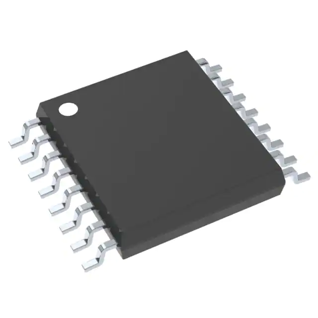
CD4042BPWE4 types contain four latch circuits, each strobed by a common clock. Complementary buffered outputs are available from each circuit. The impedance of the n- and p-channel output devices is balanced and all outputs are electrically identical.
Information present at the data input is transferred to outputs Q and Q\ during the CLOCK level which is programmed by the POLARITY input. For POLARITY = 0 the transfer occurs during the 0 CLOCK level and for POLARITY = 1 the transfer occurs during the 1 CLOCK level. The outputs follow the datainput providing the CLOCK and POLARITY levels defined above are present. When a CLOCK transition occurs (positive for POLARITY = 0 and negative for POLARITY = 1) the information present at the input during the CLOCK transition is retained at the output until an opposite CLOCK transition occurs.
The CD4042BPWE4 types are supplied in 16-lead hermetic dual-in-line ceramic packages (F3A suffixes), 16-lead dual-in-line plastic package (E suffix), 16-lead small-outline packages (D, DR, DT, DW, DWR, and NSR suffixes), and 16-lead thin shrink small-outline packages (PW and PWR suffixes).
Feature
- Clock polarity control
- Q and Q\ outputs
- Common Clock
- Low power TTL compatible
- Standardized, symmetrical output characteristics
- 100% tested for quiescent current at 20 V
- Maximum input current of 1 μA at 18 V over full package-temperature range; 100 nA at 18 V and 25°C
- 5-V, 10-V, and 15-V parametric ratings
- Noise margin (full package-temperature range) =
1 V at VDD = 5 V
2 V at VDD = 10 V
2.5 V at VDD = 15 V - Meets all requirements of JEDEC Tentative Standard No. 13B, "Standard Specifications for Description of ’B’ Series CMOS Devices"
- Applications:
- Buffer storage
- Holding register
- General digital logic


