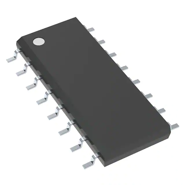
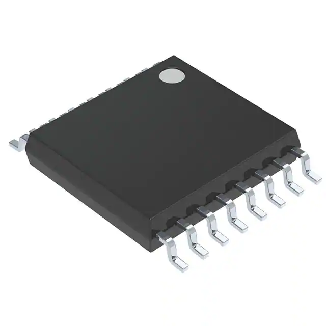
The NLV14042BDR2G Quad Transparent Latch is constructed with MOS P-channel and N-channel enhancement mode devices in a single monolithic structure. Each latch has a separate data input, but all four latches share a common clock. The clock polarity (high or low) used to strobe data through the latches can be reversed using the polarity input. Information present at the data input is transferred to outputs Q and Q during the clock level which is determined by the polarity input. When the polarity input is in the logic "0" state, data is transferred during the low clock level, and when the polarity input is in the logic "1" state the transfer occurs during the high clock level.
Feature
- Buffered Data Inputs
- Common Clock
- Clock Polarity Control
- Q and Qbar Outputs
- Double Diode Input Protection
- Supply Voltage Range = 3.0 Vdc to 1 8 Vdc
- Capable of Driving Two Low-power TTL Loads or One Low-power Schottky TTL Load Over the Rated Temperature Range
- Pb-Free Packages are Available*
(Picture: Pinout)

