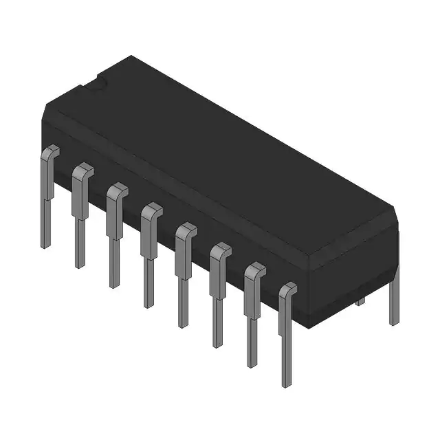
The ’HC670 and CD74HCT670E are 16-bit register files organized as 4 words x 4 bits each. Read and write address and enable inputs allow simultaneous writing into one location while reading another. Four data inputs are provided to store the 4-bit word. The write address inputs (WA0 and WA1) determine the location of the stored word in the register. When write enable (WE\) is low the word is entered into the address location and it remains transparent to the data. The outputs will reflect the true form of the input data. When (WE\) is high data and address inputs are inhibited. Data acquisition from the four registers is made possible by the read address inputs (RA1 and RA0). The addressed word appears at the output when the read enable (RE\) is low. The output is in the high impedance state when the (RE\) is high. Outputs can be tied together to increase the word capacity to 512 x 4 bits.
Feature
- Simultaneous and Independent Read and Write Operations
- Expandable to 512 Words of n-Bits
- Three-State Outputs
- Organized as 4 Words x 4 Bits Wide
- Buffered Inputs
- Typical Read Time = 16ns for ’HC670 VCC = 5V, CL = 15pF, TA = 25°C
- Fanout (Over Temperature Range)
- Standard Outputs...10 LSTTL Loads
- Bus Driver Outputs...15 LSTTL Loads
- Wide Operating Temperature Range... –55°C to 125°C
- Balanced Propagation Delay and Transition Times
- Significant Power Reduction Compared to LSTTL Logic ICs
- HC Types
- 2V to 6V Operation
- High Noise Immunity: NIL = 30%, NIH = 30% of VCC at VCC = 5V
- HCT Types
- 4.5V to 5.5V Operation
- Direct LSTTL Input Logic Compatibility, VIL = 0.8V (Max), VIH = 2V (Min)
- CMOS Input Compatibility, Il ≤ 1μA at VOL, VOH
The ’HC670 and CD74HCT670 are 16-bit register files organized as 4 words x 4 bits each. Read and write address and enable inputs allow simultaneous writing into one location while reading another. Four data inputs are provided to store the 4-bit word. The write address inputs (WA0 and WA1) determine the location of the stored word in the register. When write enable (WE\) is low the word is entered into the address location and it remains transparent to the data. The outputs will reflect the true form of the input data. When (WE\) is high data and address inputs are inhibited. Data acquisition from the four registers is made possible by the read address inputs (RA1 and RA0). The addressed word appears at the output when the read enable (RE\) is low. The output is in the high impedance state when the (RE\) is high. Outputs can be tied together to increase the word capacity to 512 x 4 bits.


