
The LM5164DDAR synchronous buck converter isdesigned to regulate over a wide input voltage range, minimizing the need for external surgesuppression components. A minimum controllable on-time of 50 ns facilitates large step-downconversion ratios, enabling the direct step-down from a 48-V nominal input to low-voltage rails forreduced system complexity and solution cost. The LM5164DDAR operates during input voltage dips as low as 6 V, at nearly 100%duty cycle if needed, making it an excellent choice for wide inputsupply range industrial and high cell count battery pack applications.
With integrated high-side and low-side power MOSFETs, the LM5164DDAR delivers up to1-A of outputcurrent. A constant on-time (COT) control architecture provides nearly constant switching frequencywith excellent load and line transient response. Additional features of the LM5164DDAR include ultra-lowIQ and diode emulation mode operation for high light-load efficiency,innovative peak and valley overcurrent protection, integrated VCC bias supply and bootstrap diode,precision enable and input UVLO, and thermal shutdown protection with automatic recovery. Anopen-drain PGOOD indicator provides sequencing, fault reporting, and output voltagemonitoring.
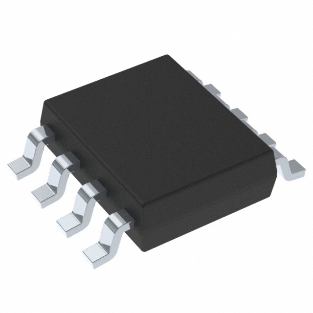
The LM5164DDAR is available in a thermally-enhanced, 8-pin SOPowerPAD package. Its 1.27-mm pin pitch providesadequate spacing for high-voltage applications.
Feature
- Designed for reliable and rugged applications
- Wide input voltage range of 6 V to 100 V
- Junction temperature range: –40°C to +150°C
- Fixed 3-ms internal soft-start timer
- Peak and valley current-limit protection
- Input UVLO and thermal shutdown protection
- Suited for scalable Industrial power supplies and battery packs
- Low minimum on- and off-times of 50 ns
- Adjustable switching frequency up to 1 MHz
- Diode emulation for high light-load efficiency
- 10.5-μA no-load input quiescent current
- 3-μA shutdown quiescent current
- Optimized for CISPR 32 EMI standard
- Integration reduces solution size and cost
- COT mode control architecture
- Integrated 0.725-Ω NFET buck switch supports wide duty-cycle range
- Integrated 0.34-Ω NFET synchronous rectifier eliminates external Schottky diode
- 1.2-V internal voltage reference
- No loop compensation components
- Internal VCC bias regulator and boot diode
- Open-drain power good indicator
- 8-Pin SOIC package with PowerPAD
- Create a custom design using WEBENCH power designer


