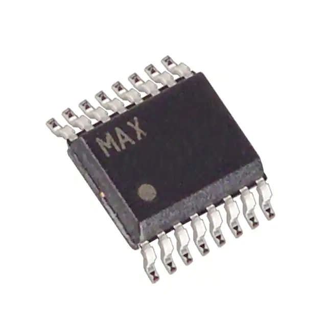
The MAX686EEE DAC-controlled boost/inverter IC converts a positive input voltage to a positive or negative LCD bias voltage up to +27.5V or -27.5V. The device features an internal N-channel MOSFET switch, programmable current limiting, and an internal 6-bit digital-to-analog converter (DAC) for digital adjustment of the output voltage. It comes in a small 16-pin QSOP package (same size as an 8-pin SO). The MAX686EEE uses a current-limited, pulse-frequency-modulation (PFM) control scheme to provide high efficiency over a wide range of load conditions. Its high switching frequency (up to 300kHz) allows the use of small external components. An LCDON output allows the LCD bias voltage to be automatically disabled when the display logic voltage is removed, protecting the display. The MAX686EEE has a +2.7V to +5.5V input voltage range for the IC, and a +0.8V to +27.5V input voltage range for the inductor. Typical quiescent supply current is 65μA. Shutdown current is 1.5μA. The MAX686EEE offers high-level integration to save space, reduce power consumption, and increase battery life, making it an excellent choice for battery-powered portable equipment. The MAX629 is similar to the MAX686, except that it does not contain a built-in DAC. Both devices have evaluation kits to facilitate designs.
Feature
- Internal 500mA, 28V N-Channel Switch (no external FET required)
- Adjustable Output Voltage to +27.5V or -27.5V
- 6-Bit DAC-Controlled Output Voltage
- Up to 90% Efficiency
- Small 16-Pin QSOP Package (Same size as 8-pin SO)
- Power-OK Indicator
- 65μA Quiescent Current
- 1.5μA Shutdown Current
- Up to 300kHz Switching Frequency
Applications
- Notebook Computers
- Palmtop Computers
- PDAs and Other Handheld Devices
- Portable Data-Collection Terminals
- Positive or Negative LCD Bias
- Varactor Tuning Diode Bias


