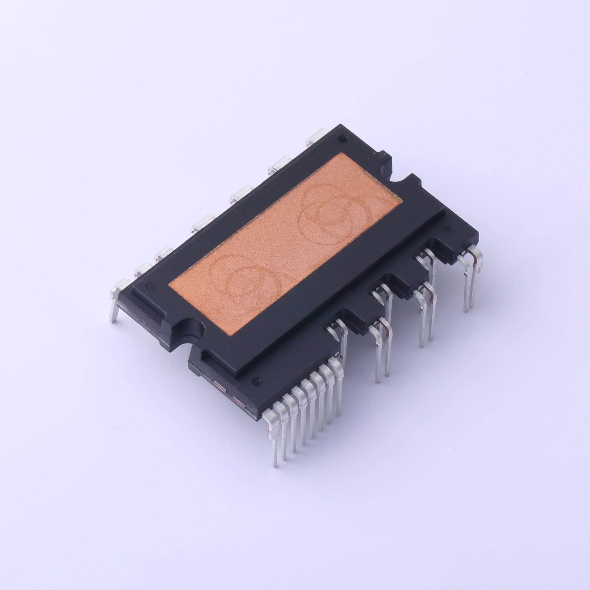
The LTC1682/LTC1682-3.3/LTC1682-5 are doubler charge pumps with an internal low noise, low dropout (LDO) linear regulator. These parts are designed to provide a low noise boosted supply voltage for powering noise sensitive devices such as high frequency VCOs in wireless applications.
An internal doubler charge pump converts a 1.8V to 4.4V input to a boosted output, while the internal LDO regulator converts the boosted voltage to a low noise regulated output. The adjustable version allows the user to set VOUT via external resistors connected to FB. The regulator is capable of supplying up to 50mA of output current. Shutdown reduces the supply current to < 5µA, removes the load from VIN by disabling the regulator and discharges VOUT to ground through a 100Ω switch.
The LTC1682IMS8 LDO regulator is stable with only 2µF on the output. Small ceramic capacitors can be used, reducing PC board area.
The LTC1682/LTC1682-3.3/LTC1682-5 are short-circuit and over temperature protected. The parts are available in 8-pin MSOP and SO packages.
Feature
- Low Output Noise: 60µVRMS (100kHz BW)
- Adjustable or Fixed Boosted Output
- Adjustable Output Voltage Range: 2.5V to 5.5V
- Fixed Output Voltages: 3.3V, 5V
- Wide Input Voltage Range: 1.8V to 4.4V
- Uses Small Ceramic Capacitors
- No Inductors Required
- Output Current up to 50mA
- 550kHz Switching Frequency
- Low Operating Current: 150µA
- Low Shutdown Current: 1µA
- Internal Thermal Shutdown and Current Limiting
- Available in 8-Pin MSOP and SO Packages
Applications
- VCO Power Supplies in Cellular Phones
- 2-Way Pagers
- Wireless PCMCIA Cards
- Portable Medical Instruments
- Low Power Data Acquisition
- Remote Transmitters


