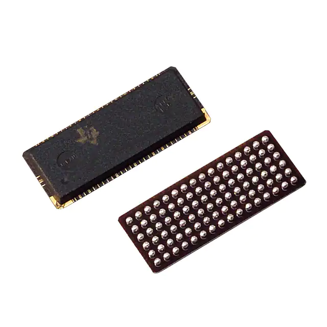
This 25-bit 1:1 or 14-bit 1:2 configurable registered buffer is designed for 1.7-V to 1.9-V VCC operation. In the 1:1 pinout configuration, only one device per DIMM is required to drive nine SDRAM loads. In the 1:2 pinout configuration, two devices per DIMM are required to drive 18 SDRAM loads.
All inputs are SSTL_18, except the reset (RESET) and control (Cn) inputs, which are LVCMOS. All outputs are edge-controlled circuits optimized for unterminated DIMM loads and meet SSTL_18 specifications.
The SN74SSTUB32864ZKER operates from a differential clock (CLK and CLK). Data are registered at the crossing of CLK going high and CLK going low.
The C0 input controls the pinout configuration of the 1:2 pinout from register-A configuration (when low) to register-B configuration (when high). The C1 input controls the pinout configuration from 25-bit 1:1 (when low) to 14-bit 1:2 (when high). C0 and C1 should not be switched during normal operation. They should be hard-wired to a valid low or high level to configure the register in the desired mode. In the 25-bit 1:1 pinout configuration, the A6, D6, and H6 terminals are driven low and are do-not-use (DNU) pins.
In the DDR2 RDIMM application, RESET is specified to be completely asynchronous with respect to CLK and CLK. Therefore, no timing relationship can be ensured between the two. When entering reset, the register is cleared, and the data outputs are driven low quickly, relative to the time required to disable the differential input receivers. However, when coming out of reset, the register becomes active quickly, relative to the time required to enable the differential input receivers. As long as the data inputs are low, and the clock is stable during the time from the low-to-high transition of RESET until the input receivers are fully enabled, the design of the SN74SSTUB32864ZKER ensures that the outputs remain low, thus ensuring there will be no glitches on the output.
To ensure defined outputs from the register before a stable clock has been supplied, RESET must be held in the low state during power up.
The device supports low-power standby operation. When RESET is low, the differential input receivers are disabled, and undriven (floating) data, clock, and reference voltage (VREF) inputs are allowed. In addition, when RESET is low, all registers are reset and all outputs are forced low, except QERR. The LVCMOS RESET and Cn inputs always must be held at a valid logic high or low level.
The device also supports low-power active operation by monitoring both system chip select (DCS and CSR) inputs and gates the Qn outputs from changing states when both DCS and CSR inputs are high. If either DCS or CSR input is low, the Qn outputs function normally. The RESET input has priority over the DCS and CSR control and, when driven low, forces the Qn outputs low. If the DCS control functionality is not desired, the CSR input can be hard-wired to ground, in which case the setup-time requirement for DCS is the same as for the other D data inputs. To control the low-power mode with DCS only, the CSR input should be pulled up to VCC through a pullup resistor.
The two VREF pins (A3 and T3) are connected together internally by approximately 150. However, it isnecessary to connect only one of the two VREF pins to the external VREF power supply. An unused VREF pin should be terminated with a VREF coupling capacitor.
Feature
- Member of the Texas Instruments Widebus+ Family
- Pinout Optimizes DDR2 DIMM PCB Layout
- Configurable as 25-Bit 1:1 or 14-Bit 1:2 Registered Buffer
- Chip-Select Inputs Gate the Data Outputs from Changing State and Minimizes SystemPower Consumption
- Output Edge-Control Circuitry Minimizes Switching Noise in an Unterminated Line
- Supports SSTL_18 Data Inputs
- Differential Clock (CLK and CLK) Inputs
- Supports LVCMOS Switching Levels on the Control and RESET Inputs
- Supports Industrial Temperature Range (-40°C to 85°C)
- RESET Input Disables Differential Input Receivers, Resets All Registers, and Forces All Outputs Low


