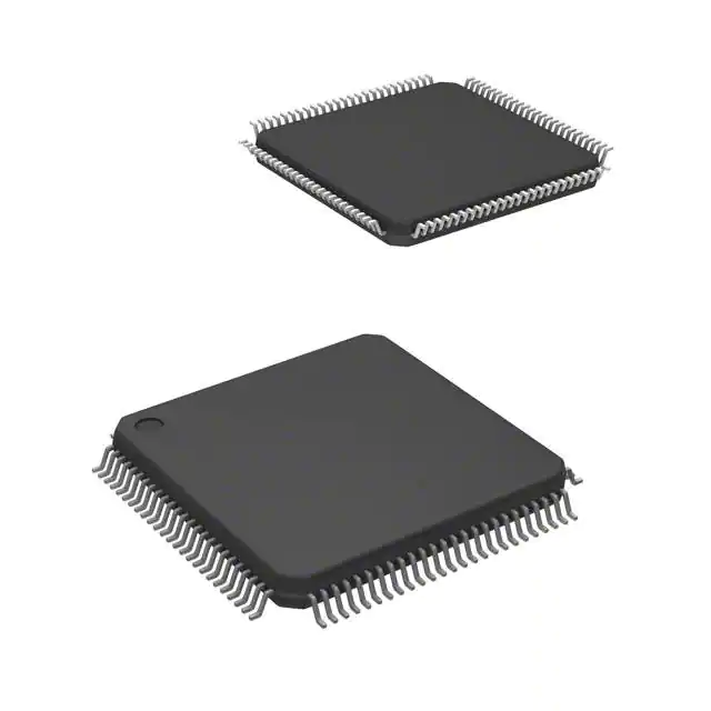
The SN74FB1653PCA contains an 8-bit and a 9-bit transceiver with a buffered clock. The clock and transceivers are designed to translate signals between LVTTL and BTL environments. The device is designed specifically to be compatible with IEEE Std 1194.1-1991 (BTL).
The A port operates at LVTTL signal levels. The A outputs reflect the inverse of the data at the B\ port when the A-port output enable (OEA) is high. When OEA is low or when VCC(5 V) typically is less than 2.5 V, the A outputs are in the high-impedance state.
The B\ port operates at BTL signal levels. The open-collector B\ ports are specified to sink 100 mA. Two output enables (OEB and OEB)\ are provided for the B\ outputs. When OEB is low, OEB\ is high, or VCC(5 V) typically is less than 2.5 V, the B port is turned off.
The clock-select (2SEL1 and 2SEL2) inputs are used to configure the TTL-to-BTL clock paths and delays (refer to the MUX-MODE DELAY table).
BIAS VCC establishes a voltage between 1.62 V and 2.1 V on the BTL outputs when VCC(5 V) is not connected.
BG VCC and BG GND are the supply inputs for the bias generator.
VREF is an internally generated voltage source. It is recommended that VREF be decoupled with a 0.1-μF capacitor.
Enhanced heat-dissipation techniques should be used when operating this device from AI to A0 at frequencies greater than 50 MHz, or from AI to B\ or B\ to A0 at frequencies greater than 100 MHz.
Feature
- Compatible With IEEE Std 1194.1-1991 (BTL)
- LVTTL A Port, Backplane Transceiver Logic (BTL) B\ Port
- Open-Collector B\-Port Outputs Sink 100 mA
- B\-Port Biasing Network Preconditions the Connector and PC Trace to the BTL High-Level Voltage
- High-Impedance State During Power Up and Power Down
- Selectable Clock Delay
- TTL-Input Structures Incorporate Active Clamping Networks to Aid in Line Termination
- BIAS VCC Minimizes Signal Distortion During Live Insertion/Withdrawal
The SN74FB1653 contains an 8-bit and a 9-bit transceiver with a buffered clock. The clock and transceivers are designed to translate signals between LVTTL and BTL environments. The device is designed specifically to be compatible with IEEE Std 1194.1-1991 (BTL).
The A port operates at LVTTL signal levels. The A outputs reflect the inverse of the data at the B\ port when the A-port output enable (OEA) is high. When OEA is low or when VCC(5 V) typically is less than 2.5 V, the A outputs are in the high-impedance state.
The B\ port operates at BTL signal levels. The open-collector B\ ports are specified to sink 100 mA. Two output enables (OEB and OEB)\ are provided for the B\ outputs. When OEB is low, OEB\ is high, or VCC(5 V) typically is less than 2.5 V, the B port is turned off.
The clock-select (2SEL1 and 2SEL2) inputs are used to configure the TTL-to-BTL clock paths and delays (refer to the MUX-MODE DELAY table).
BIAS VCC establishes a voltage between 1.62 V and 2.1 V on the BTL outputs when VCC(5 V) is not connected.
BG VCC and BG GND are the supply inputs for the bias generator.
VREF is an internally generated voltage source. It is recommended that VREF be decoupled with a 0.1-μF capacitor.
Enhanced heat-dissipation techniques should be used when operating this device from AI to A0 at frequencies greater than 50 MHz, or from AI to B\ or B\ to A0 at frequencies greater than 100 MHz.


