· Provides Level Translation From LVDS or LVPECL to CML, Repeating From CML to CML
· Signaling Rates(1) up to 1.5 Gbps
· CML Compatible Output Directly Drives Devices With 3.3-V,2.5-V, or 1.8-V Supplies
· Total Jitter<70 ps
· Low 100 ps(Max) Part-To-Part Skew
· Wide Common-Mode Receiver Capability Allows Direct Coupling of Input Signals
·25 mV of Receiver Input Threshold Hysteresis Over 0-V to 4-V Common-Mode Range
· Propagation Delay Times,800 ps Maximum
·3.3-V Supply Operation
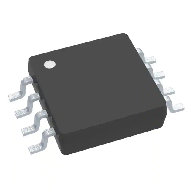
· Available in SOIC and MSOP Packages
APPLICATIONS
·Level Translation
·622-MHz Central Office Clock Distribution
·High-Speed Network Routing
·Wireless Basestations
·Low Jitter Clock Repeater
DESCRIPTION
This high-speed translator/repeater is designed for signaling rates up to 1.5 Gbps to support various high-speed network routing applications. The driveroutput is compatible with current-mode logic (CML)
levels, and directly drives 50-2 or 25-2 loads connected to 1.8-V,2.5-V, or 3.3-V nominal supplies.
The capability for direct connection to the loads may eliminate the need for coupling capacitors. The receiver input is compatible with LVDS(TIA/EIA-644), LVPECL, and CML signaling levels. The receiver tolerates a wide common-mode voltage range, and may also be directly coupled to the signal source.The internal data path from input to output is fully differential for low noise generation and low pulse-width distortion.
The VBB pin is an internally generated voltage supply to allow operation with a single-ended LVPECL input.
For single-ended LVPECL input operation, the unused differential input is connected to VeB as a switching reference voltage. When used, decouple VeB with a 0.01-uF capacitor and limit the current sourcing or sinking to 400 uA. When not used, VBB should be left open.
This device is characterized for operation from-40℃ to 85℃.
(Picture:Pinout / Diagram)


