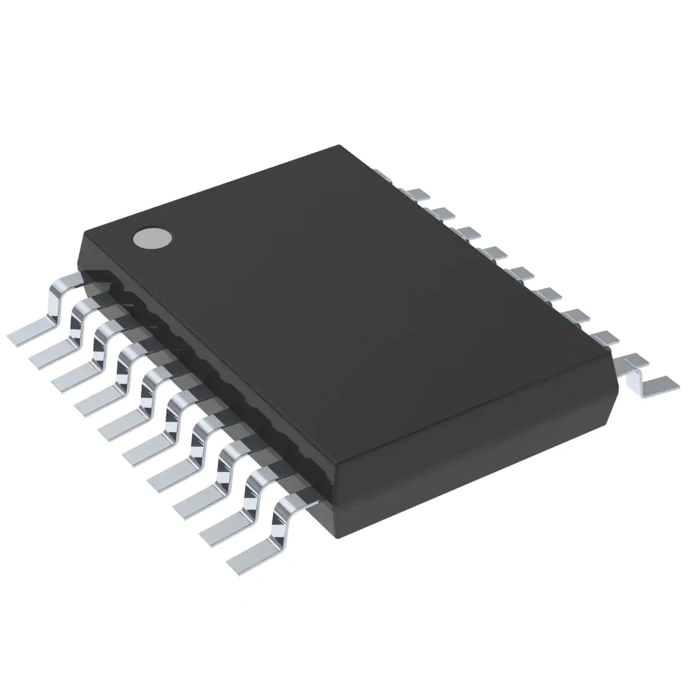
The SN74GTLP817DW is a medium-drive fanout driver that provides LVTTL-to-GTLP and GTLP-to-LVTTL signal-level translation. The device provides a high-speed interface between cards operating at LVTTL logic levels and a backplane operating at GTLP signal levels. High-speed (about three times faster than standard TTL or LVTTL) backplane operation is a direct result of GTLP reduced output swing (<1 V), reduced input threshold levels, improved differential input, and OEC circuitry. The improved GTLP OEC circuitry minimizes bus settling time and has been designed and tested using several backplane models. The medium drive allows incident-wave switching in heavily loaded backplanes with equivalent load impedance down to 19 . BO1 and BO2 can be tied together to drive an equivalent load impedance down to 11 .
GTLP is the Texas Instruments (TI) derivative of the Gunning Transceiver Logic (GTL) JEDEC standard JESD 8-3. The ac specification of the SN74GTLP817DW is given only at the preferred higher noise-margin GTLP, but the user has the flexibility of using this device at either GTL (VTT = 1.2 V and V REF = 0.8 V) or GTLP (VTT = 1.5 V and VREF = 1 V) signal levels.
Normally, the B port operates at GTLP signal levels. The A-port and control inputs operate at LVTTL logic levels but are 5-V tolerant and are compatible with TTL and 5-V CMOS inputs. VREF is the B-port differential input reference voltage.
GNDT is the TTL output ground, while GNDG is the GTLP output ground, and both may be separated from each other for a quieter device.
This device is fully specified for hot-insertion applications using Ioff and power-up 3-state. The Ioff circuitry disables the outputs, preventing damaging current backflow through the device when it is powered down. The power-up 3-state circuitry places the outputs in the high-impedance state during power up and power down, which prevents driver conflict.
This device features adjustable edge-rate control (ERC). Changing the ERC input voltage between GND and VCC adjusts the B-port output rise and fall times. This allows the designer to optimize system data-transfer rate and signal integrity to the backplane load. ERC automatically is selected to the same speed as alternate source 1-to-6 fanout drivers that use pin 18 for 3.3-V or 5-V VCC .
When VCC is between 0 and 1.5 V, the device is in the high-impedance state during power up or power down. However, to ensure the high-impedance state above 1.5 V, the output-enable (OE\) input should be tied to VCC through a pullup resistor; the minimum value of the resistor is determined by the current-sinking capability of the driver.
Feature
- OEC Circuitry Improves Signal Integrity and Reduces Electromagnetic Interference
- Bidirectional Interface Between GTLP Signal Levels and LVTTL Logic Levels
- GTLP-to-LVTTL 1-to-6 Fanout Driver
- LVTTL-to-GTLP 1-to-2 Fanout Driver
- LVTTL Interfaces Are 5-V Tolerant
- Medium-Drive GTLP Outputs (50 mA)
- Reduced-Drive LVTTL Outputs (\x9612 mA/12 mA)
- Variable Edge-Rate Control (ERC) Input Selects GTLP Rise and Fall Times for Optimal Data-Transfer Rate and Signal Integrity in Distributed Loads
- Ioff and Power-Up 3-State Support Hot Insertion
- Distributed VCC and GND Pins Minimize High-Speed Switching Noise
- Latch-Up Performance Exceeds 100 mA Per JESD 78, Class II
- ESD Protection Exceeds JESD 22
- 2000-V Human-Body Model (A114-A)
- 200-V Machine Model (A115-A)
- 1000-V Charged-Device Model (C101)


