All trademarks are the property of their respective owners.
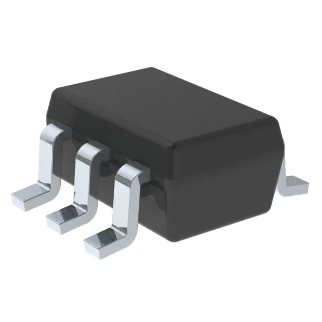
DescriptionThe SN74AXC1T45DBVR is a single-bit noninverting bustransceiver that uses two separate configurable power-supply rails. The device is operational withboth VCCA and VCCB supplies as low as 0.65 V. The Aport is designed to track VCCA, which accepts any supply voltage from 0.65 Vto 3.6 V. The B port is designed to track VCCB, which also accepts anysupply voltage from 0.65 V to 3.6 V.
The DIR pin determines the direction of signal propagation. With the DIR pin configuredHIGH, translation is from Port A to Port B. With DIR configured LOW, translation is from Port B toPort A. The DIR pin is referenced to VCCA, meaning that its logic-high andlogic-low thresholds track with VCCA.
This device is fully specified for partial-power-down applications using theIoff current. The Ioff protection circuitry ensuresthat no excessive current is drawn from or to an input, output, or combined I/O that is biased to aspecific voltage while the device is powered down.
The VCC isolation feature ensures that if eitherVCCA or VCCB is less than 100 mV, both I/O portsenter a high-impedance state by disabling their outputs.
The glitch suppression circuitry enables either supply rail to be powered on or off inany order, providing robust power sequencing performance.
Feature
- Up and Down Translation Across 0.65 V to 3.6 V
- Operating Temperature: –40°C to +125°C
- Designed with glitch suppression circuitry to improve power sequencingperformance
- Maximum Quiescent Current (ICCA +ICCB) of 6 μA (85°C Maximum) and 14 μA (125°C Maximum)
- Up to 500-Mbps Support When Translating from 1.8 to3.3V
- VCC Isolation Feature
- If Either VCC Input is Below 100 mV, All I/Os Outputsare Disabled and Become High-Impedance
- Ioff Supports Partial-Power-Down Mode Operation
- Latch-Up Performance Exceeds 100 mA Per JESD 78, Class II
- ESD Protection Exceeds JESD 22
- 8000-V Human Body Model
- 1000-V Charged-DeviceModel
All trademarks are the property of their respective owners.
DescriptionThe SN74AXC1T45 is a single-bit noninverting bustransceiver that uses two separate configurable power-supply rails. The device is operational withboth VCCA and VCCB supplies as low as 0.65 V. The Aport is designed to track VCCA, which accepts any supply voltage from 0.65 Vto 3.6 V. The B port is designed to track VCCB, which also accepts anysupply voltage from 0.65 V to 3.6 V.
The DIR pin determines the direction of signal propagation. With the DIR pin configuredHIGH, translation is from Port A to Port B. With DIR configured LOW, translation is from Port B toPort A. The DIR pin is referenced to VCCA, meaning that its logic-high andlogic-low thresholds track with VCCA.
This device is fully specified for partial-power-down applications using theIoff current. The Ioff protection circuitry ensuresthat no excessive current is drawn from or to an input, output, or combined I/O that is biased to aspecific voltage while the device is powered down.
The VCC isolation feature ensures that if eitherVCCA or VCCB is less than 100 mV, both I/O portsenter a high-impedance state by disabling their outputs.
The glitch suppression circuitry enables either supply rail to be powered on or off inany order, providing robust power sequencing performance.


