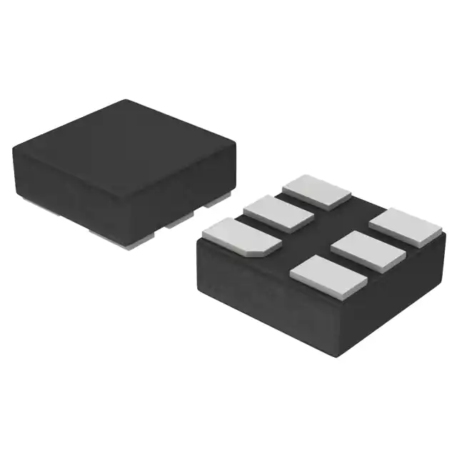
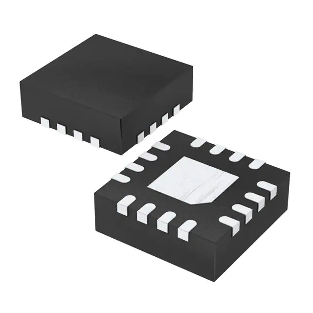
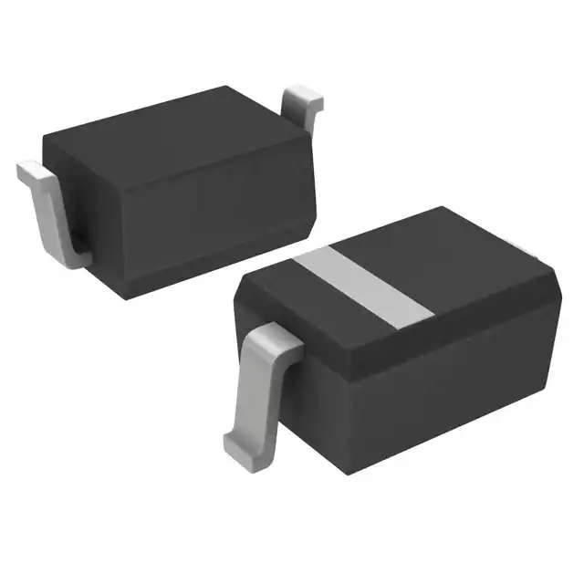
The NLSX5011AMX1TCG is a 1-bit configurable dual-supply autosensing bidirectional level translator that does not require a direction control pin. The IO VCC- and IO VL- ports are designed to track two different power supply rails, VCC and VL respectively. Both the VCC and the VL supply rails are configurable from 0.9 V to 4.5 V. This allows a logic signal on the VL side to be translated to either a higher or a lower logic signal voltage on the VCC side, adn vice-versa. The NLSX5011AMX1TCG offers the feature that the values of the VCC and VL supplies are independent. Design flexibility is maximized because VL can be set to a value either greater than or less than the VCC supply. In contrast, the majority of competitive auto sense translators have a restriction that the value of the VL supply must be equal to less than (VCC - 0.4) V. The NLSX5011AMX1TCG has high output current capability, which allows the translator to drive high capacitive loads such as most high freequency EMI filters. Another feature of the NLSX5011AMX1TCG is that each IO_VLn and IO_VCCn channel can function as either an input or an output. An Output Enable (EN) input is available to reduce the power consumption. The EN pin can be used to disable both IO ports by putting them in 3-state which significantly reduces the supply current from both VCC and VL. The EN signal is referenced to the VL supply.
Feature
- Wide VCC, VL Operating Range: 0.9 V to 4.5 V
- VL and VCC are independent. VL may be greater than, equal to, or less than VCC
- High 100 pF Capacitive Drive Capability
- HighSpeed with 140 Mb/s Guaranteed Date Ratefor VCC, VL > 1.8 V
- Low Bit to Bit Skew
- Overvoltage Tolerant Enable and I/O Pins
- Nonpreferential Power Up Sequencing
- Power Off Protection
- Small packaging; UDFN-6 (1.45mm x 1.0mm) and (1.2mm x 1.0mm)
- These are PbFree devices
Applications
- Mobile Phones, PDAs, Other Portable Devices


