General Description
The MAX5090A/B/C easy-to-use, high-efficiency, highvoltage step-down DC-DC converters operate from an input voltage up to 76V, and consume only 310µA quiescent current at no load. This pulse-width-modulated (PWM) converter operates at a fixed 127kHz switching frequency at heavy loads, and automatically switches to pulse-skipping mode to provide low quiescent current and high efficiency at light loads. The MAX5090 includes internal frequency compensation simplifying circuit implementation. The device can also be synchronized with external system clock frequency in a noise-sensitive application. The MAX5090 uses an internal low on-resistance and a high-voltage DMOS transistor to obtain high efficiency and reduce overall system cost. This device includes undervoltage lockout, cycle-by-cycle current limit, hiccup-mode output short-circuit protection, and overtemperature shutdown. The MAX5090 delivers up to 2A output current. External shutdown is included, featuring 19µA (typ) shutdown current. The MAX5090A/MAX5090B versions have fixed output voltages of 3.3V and 5V, respectively, while the MAX5090C features an adjustable 1.265V to 11V output voltage. The MAX5090 is available in a space-saving 16-pin thin QFN package (5mm x 5mm) and operates over the automotive temperature range (-40°C to +125°C).
Features
♦ Wide Input Voltage Range: 6.5V to 76V
♦ Fixed (3.3V, 5V) and Adjustable (1.265V to 11V) Output-Voltage Versions
♦ 2A Output Current
♦ Efficiency Up to 92%
♦ Internal 0.26Ω High-Side DMOS FET
♦ 310µA Quiescent Current at No Load
♦ 19µA Shutdown Current
♦ Internal Frequency Compensation
♦ Fixed 127kHz Switching Frequency
♦ External Frequency Synchronization
♦ Thermal Shutdown and Short-Circuit Current Limit
♦ -40°C to +125°C Automotive Temperature Range
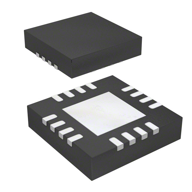
♦ 16-Pin (5mm x 5mm) Thin QFN Package
♦ Capable of Dissipating 2.67W at +70°C
Feature
- Single +5V or Dual ±5V Supply Operation
- Output Buffer Amplifiers Swing Rail-to-Rail
- Reference Input Range Includes Both Supply Rails
- Calibrated Offset, Gain, and Linearity (1 LSB TUE)
- 10MHz Serial Interface, Compatible with SPI, QSPI (CPOL = CPHA = 0) and Microwire
- Double-Buffered Registers for Synchronous Updating
- Serial Data Output for Daisy-Chaining
- Power-On Reset Clears Serial Interface and Sets All Registers to Zero
Applications
- Digital Attenuator
- Digital Gain and Offset Control
- General Purpose
(Picture: Pinout)


