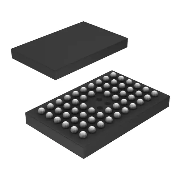
The ’LVTH16500 devices are 18-bit universal bus transceivers designed for low-voltage (3.3-V) VCC operation, but with the capability to provide a TTL interface to a 5-V system environment.
Data flow in each direction is controlled by output-enable (OEAB and OEBA\), latch-enable (LEAB and LEBA), and clock (CLKAB\ and CLKBA\) inputs. For A-to-B data flow, the devices operate in the transparent mode when LEAB is high. When LEAB is low, the A data is latched if CLKAB\ is held at a high or low logic level. If LEAB is low, the A data is stored in the latch/flip-flop on the high-to-low transition of CLKAB\. OEAB is active high. When OEAB is high, the B-port outputs are active. When OEAB is low, the B-port outputs are in the high-impedance state.
Data flow for B to A is similar to that of A to B but uses OEBA\, LEBA, and CLKBA\. The output enables are complementary (OEAB is active high and OEBA\ is active low).
Active bus-hold circuitry holds unused or undriven inputs at a valid logic state. Use of pullup or pulldown resistors with the bus-hold circuitry is not recommended.
When VCC is between 0 and 1.5 V, the devices are in the high-impedance state during power up or power down. However, to ensure the high-impedance state above 1.5 V, (OE)\ should be tied to VCC through a pullup resistor and OE should be tied to GND through a pulldown resistor; the minimum value of the resistor is determined by the current-sinking/current-sourcing capability of the driver.
These devices are fully specified for hot-insertion applications using Ioff and power-up 3-state. The Ioff circuitry disables the outputs, preventing damaging current backflow through the devices when they are powered down. The power-up 3-state circuitry places the outputs in the high-impedance state during power up and power down, which prevents driver conflict.
Feature
- Members of the Texas Instruments Widebus Family
- UBT Transceivers Combine D-Type Latches and D-Type Flip-Flops for Operation in Transparent, Latched, or Clocked Mode
- Support Mixed-Mode Signal Operation (5-V Input and Output Voltages With 3.3-V VCC)
- Support Unregulated Battery Operation Down to 2.7 V
- Typical VOLP (Output Ground Bounce)
<0.8 V at VCC = 3.3 V, TA = 25°C - Ioff and Power-Up 3-State Support Hot Insertion
- Bus Hold on Data Inputs Eliminates the Need for External Pullup/Pulldown Resistors
- Distributed VCC and GND Pins Minimize High-Speed Switching Noise
- Flow-Through Architecture Optimizes PCB Layout
- Latch-Up Performance Exceeds 500 mA Per JESD 17
- ESD Protection Exceeds JESD 22
- 2000-V Human-Body Model (A114-A)
- 200-V Machine Model (A115-A)
- 1000-V Charged-Device Model (C101)


