FEATURES
·2-Bit Bidirectional Translator for SDA and SCL Lines in Mixed-Mode 12C Applications
·5.5-V Tolerant OE Input· Level Translation Range
-1.8 V to 2.5V/3.3VI5V
-2.5V to 2.5V/3.3VI5V
-3.3Vto 3.3V/5V
· Internal10-kQ Pullup Resistor on Each Port and Option to Add External Pullup Resistor if Required
· Provides Bidirectional Voltage Translation With No Direction Pin
· lof Support Partial Power Down (Vcc=0V)
With 2 mA
· High-lmpedance Output SCL1, SDA1, SCL2, and SDA2 Pins When OE=Low or Vcc=0V
· Latch-Up Performance Exceeds 100 mA Per JESD 78, Class ll
· ESD Protection Exceeds JESD 22
-A Port
-2500-V Human-Body Model(A114-B)
-250-V Machine Model (A115-A)
-1500-V Charged-Device Model(C101)
-BPort
-8-kV Human-Body Model(A114-B)
-250-V Machine Model (A115-A)
-1500-VCharged-Device Model(C101)
TYPICAL LEVEL-SHIFTER
APPLICATIONS
·1PC/SMBus
·UART
·GPIO
DESCRIPTION
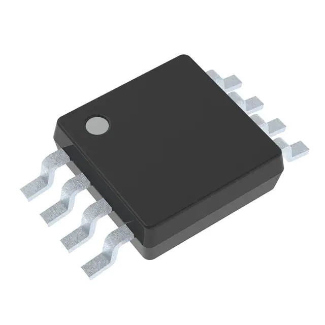
The TCA9406DCUR is a dual bidirectional I 2C-Bus and SMBus Voltage-Level translator with enable (OE) Input.
It is operational from 1.65 V to 3.6 V on A-Port and 2.3 V to 5.5 V on B-port.
The Output Enable (OE) input is referenced to VCCA, but is 5.5V tolerant The device can also be used as a general purpose level-translator, supporting push-pull driving of the A and B ports.
When driven with push-pull devices on both sides the TCA9406DCUR can support up to 24Mps.
Under normal I2C and SMBus operation or other open drain configurations, the device can support up to 2Mbps.
It is compatible with a standard I 2C bus 100 kHz, 400 kHz and 1 MHz at both sides of A-Port and BPort.
The TCA9406DCUR features internal 10kOHM pullup resistors.
Additional external pullup resistors can be added to the bus to reduce total pullup resistance.
Feature
- 2-Bit Bidirectional Translator for SDA and SCL Lines in I2CApplications
- Provides Bidirectional Voltage Translation With No DirectionPin
- High-Impedance Output SCL_A, SDA_A, SCL_B, SDA_B Pins When OE = Low orVCC = 0 V
- Internal 10-kΩ Pullup Resistor on All SDA andSCL Pins
- 1.65 V to 3.6 V on A port and 2.3 V to 5.5 V on B port (VCCA≤ VCCB)
- VCC Isolation Feature: If Either VCCInput Is at GND, Both Ports Are in the High-Impedance State
- No Power-Supply Sequencing Required: Either VCCA orVCCB Can Be Ramped First
- Low Ioff of 2 μA When Either VCCA orVCCB = 0 V
- OE Input Can Be Tied Directly toVCCA Or Controlled By GPIO
- Latch-Up Performance Exceeds 100 mA Per JESD 78, Class II
- ESD Protection Exceeds JESD 22
- A Port
- 2500-V Human-Body Model (A114-B)
- 250-V Machine Model (A115-A)
- 1500-V Charged-Device Model (C101)
- B Port
- 8-kV Human-Body Model (A114-B)
- 250-V Machine Model (A115-A)
- 1500-V Charged-Device Model (C101)
- A Port
All trademarks are the property of their respective owners.
(Picture: Pinout)

