All trademarks are the property of their respective owners.
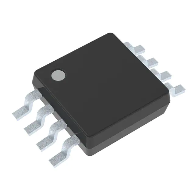
DescriptionThis 2-bit non-inverting bus transceiver uses two separate configurable power-supplyrails. The A ports are designed to track VCCA and accepts any supply voltagefrom 1.2 V to 3.6 V. The B ports are designed to track VCCB and accepts anysupply voltage from 1.2 V to 3.6 V. This allows for universal low-voltage bidirectional translationand level-shifting between any of the 1.2-V, 1.5-V, 1.8-V, 2.5-V, and 3.3-V voltage nodes.
The SN74AVC2T45DCUT is designed for asynchronous communication between two data buses. Thelogic levels of the direction-control (DIR pin) input activate either the B-port outputs or theA-port outputs. The device transmits data from the A bus to the B bus when the B-port outputs areactivated and from the B bus to the A bus when the A-port outputs are activated. The inputcircuitry on both A and B ports always is active and must have a logic HIGH or LOW level applied toprevent excess leakage current on the internal CMOS structure.
Feature
- Available in the Texas Instruments NanoFree? Package
- VCC Isolation Feature: If Either VCCInput Is at GND, Both Ports Are in the High-Impedance State
- Dual Supply Rail Design
- I/Os Are 4.6-V Over Voltage Tolerant
- Ioff Supports Partial-Power-Down Mode Operation
- Max Data Rates
- 500 Mbps (1.8 V to 3.3 V)
- 320 Mbps (<1.8 V to 3.3 V )
- 320 Mbps (Level-Shifting to 2.5 V or 1.8 V)
- 280 Mbps (Level-Shifting to 1.5 V)
- 240 Mbps (Level-Shifting to 1.2 V)
- Latch-Up Performance Exceeds 100 mA Per JESD 78, Class II
- ESD Protection Exceeds JESD 22
All trademarks are the property of their respective owners.
DescriptionThis 2-bit non-inverting bus transceiver uses two separate configurable power-supplyrails. The A ports are designed to track VCCA and accepts any supply voltagefrom 1.2 V to 3.6 V. The B ports are designed to track VCCB and accepts anysupply voltage from 1.2 V to 3.6 V. This allows for universal low-voltage bidirectional translationand level-shifting between any of the 1.2-V, 1.5-V, 1.8-V, 2.5-V, and 3.3-V voltage nodes.
The SN74AVC2T45 is designed for asynchronous communication between two data buses. Thelogic levels of the direction-control (DIR pin) input activate either the B-port outputs or theA-port outputs. The device transmits data from the A bus to the B bus when the B-port outputs areactivated and from the B bus to the A bus when the A-port outputs are activated. The inputcircuitry on both A and B ports always is active and must have a logic HIGH or LOW level applied toprevent excess leakage current on the internal CMOS structure.


