All trademarks are the property of their respective owners.
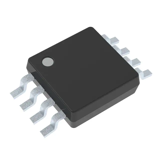
DescriptionThe TXB0102DCUT device is a 2-bit noninverting translator that uses two separate configurablepower-supply rails. The A port is designed to track VCCA.VCCA accepts any supply voltage from 1.2 V to 3.6 V. The B port is designedto track VCCB. VCCB accepts any supply voltage from1.65 V to 5.5 V. This allows for universal low-voltage bidirectional translation between any of the1.2-V, 1.5-V, 1.8-V, 2.5-V, 3.3-V, and 5-V voltage nodes. VCCA must notexceed VCCB.
When the output-enable (OE) input is low, all outputs are placed in the high-impedancestate.
This device is fully specified for partial-power-down applications usingIoff. The Ioff circuitry disables the outputs whenthe device is powered down. This inhibits current backflow into the device which prevents damage tothe device.
OE must be tied to GND through a pulldown resistor to assure the high-impedance stateduring power up or power down; the minimum value of the resistor is determined by thecurrent-sourcing capability of the driver.
NanoFree? technology is a major breakthrough in IC packaging concepts, using the die asthe package.
Feature
- Available in the Texas Instruments NanoFree? Packages
- 1.2 V to 3.6 V on A Port and 1.65 V to 5.5 V OnB Port (VCCA≤ VCCB)
- VCC Isolation Feature – If Either VCCInput Is at GND, All Outputs Are in the High-Impedance State
- OE Input Circuit Referenced to VCCA
- Low Power Consumption, 4-μA Max ICC
- Ioff Supports Partial-Power-Down Mode Operation
- Latch-Up Performance Exceeds 100 mA Per JESD 78, Class II
- ESD Protection Exceeds JESD 22
- APort
- 2500-V Human-Body Model (A114-B)
- 200-V Machine Model (A115-A)
- 1500-V Charged-Device Model (C101)
- B Port
- 15-kV Human-Body Model (A114-B)
- 200-V Machine Model (A115-A)
- 1500-V Charged-Device Model (C101)
- APort
All trademarks are the property of their respective owners.
DescriptionThe TXB0102 device is a 2-bit noninverting translator that uses two separate configurablepower-supply rails. The A port is designed to track VCCA.VCCA accepts any supply voltage from 1.2 V to 3.6 V. The B port is designedto track VCCB. VCCB accepts any supply voltage from1.65 V to 5.5 V. This allows for universal low-voltage bidirectional translation between any of the1.2-V, 1.5-V, 1.8-V, 2.5-V, 3.3-V, and 5-V voltage nodes. VCCA must notexceed VCCB.
When the output-enable (OE) input is low, all outputs are placed in the high-impedancestate.
This device is fully specified for partial-power-down applications usingIoff. The Ioff circuitry disables the outputs whenthe device is powered down. This inhibits current backflow into the device which prevents damage tothe device.
OE must be tied to GND through a pulldown resistor to assure the high-impedance stateduring power up or power down; the minimum value of the resistor is determined by thecurrent-sourcing capability of the driver.
NanoFree? technology is a major breakthrough in IC packaging concepts, using the die asthe package.

