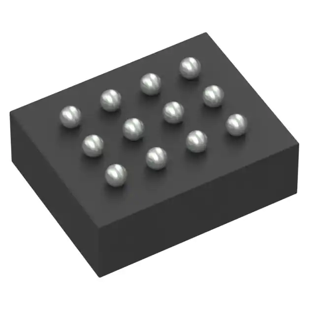
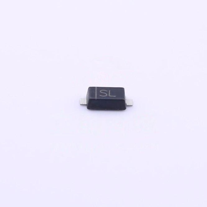
This TXB0104AD 4-bit noninverting translator uses two separate configurable power-supplyrails. The A port is designed to track VCCA. VCCAaccepts any supply voltage from 1.2 V to 3.6 V. The B port is designed to trackVCCB. VCCB accepts any supply voltage from 1.65 V to5.5 V. This allows for universal low-voltage bidirectional translation between any of the 1.2-V,1.5-V, 1.8-V, 2.5-V, 3.3-V, and 5-V voltage nodes. VCCA must not exceedVCCB.
When the OE input is low, all outputs are placed in the high-impedance state. To ensurethe high-impedance state during power up or power down, OE must be tied to GND through a pulldownresistor The current sourcing capability of the driver determines the minimum value of theresistor.
The TXB0104AD device is designed so the OE input circuit is supplied byVCCA.
This device is fully specified for partial power-down applications using IOFF. The I OFF circuitry disables the outputs, which preventsdamaging current backflow through the device when the device is powered down.
Feature
- 1.2-V to 3.6-V on A Port and 1.65-V to 5.5-V
on B Port (VCCA ≤ VCCB) - VCC Isolation Feature: If Either VCC Input Is at GND, All Outputs Are in the High-Impedance State
- Output Enable (OE) Input Circuit Referenced to VCCA
- Low Power Consumption, 5-μA Maximum ICC
- I OFF Supports Partial Power-Down Mode Operation
- Latch-Up Performance Exceeds 100 mA Per JESD 78, Class II
- ESD Protection Exceeds JESD 22
- A Port:
- 2500-V Human-Body Model (A114-B)
- 1500-V Charged-Device Model (C101)
- B Port:
- ±15-kV Human-Body Model (A114-B)
- 1500-V Charged-Device Model (C101)
- A Port:

