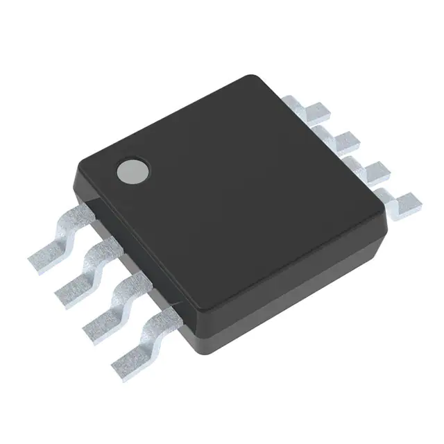
This dual bidirectional I2C and SMBus voltage-level translator, with an enable (EN) input, is operational from 1.2-V to 3.3-V VREF1 and 1.8-V to 5.5-V VREF2.
The PCA9306-Q1 allows bidirectional voltage translations between 1.2 V and 5 V, without the use of a direction pin. The low ON-state resistance (ron) of the switch allows connections to be made with minimal propagation delay. When EN is high, the translator switch is ON, and the SCL1 and SDA1 I/O are connected to the SCL2 and SDA2 I/O, respectively, allowing bidirectional data flow between ports. When EN is low, the translator switch is off, and a high-impedance state exists between ports.
In I2C applications, the bus capacitance limit of 400 pF restricts the number of devices and bus length. Using the PCA9306-Q1 enables the system designer to isolate two halves of a bus; thus, more I2C devices or longer trace length can be accommodated.
The PCA9306-Q1 also can be used to run two buses, one at 400-kHz operating frequency and the other at 100-kHz operating frequency. If the two buses are operating at different frequencies, the 100-kHz bus must be isolated when the 400-kHz operation of the other bus is required. If the master is running at 400 kHz, the maximum system operating frequency may be less than 400 kHz because of the delays added by the repeater.
All channels have the same electrical characteristics, and there is minimal deviation from one output to another in voltage or propagation delay. This is a benefit over discrete transistor voltage translation solutions, because the fabrication of the switch is symmetrical. The translator provides excellent ESD protection to lower-voltage devices and at the same time protects less ESD-resistant devices.
Feature
- Qualified for Automotive Applications
- AEC-Q100 Qualified With the Following Results:
- Device Temperature Grade 2: –40°C to 105°C
- Device HBM ESD Classification Level H2
- Device CDM ESD Classification Level C4B
- 2-Bit Bidirectional Translator for SDA and SCL Lines in Mixed-Mode I2C Applications
- Compatible With I2C and SMBus
- Less Than 1.5-ns Maximum Propagation Delay to Accommodate Standard-Mode and Fast-Mode I2C Devices and Multiple Masters
- Allows Voltage-Level Translation Between
- 1.2-V VREF1 and 1.8-V, 2.5-V, 3.3-V, or 5-V VREF2
- 1.8-V VREF1 and 2.5-V, 3.3-V, or 5-V VREF2
- 2.5-V VREF1 and 3.3-V, or 5-V VREF2
- 3.3-V VREF1 and 5-V VREF2
- Provides Bidirectional Voltage Translation With No Direction Pin
- Low 3.5-Ω ON-State Connection Between Input and Output Ports Provides Less Signal Distortion
- Open-Drain I2C I/O Ports (SCL1, SDA1, SCL2, and SDA2)
- 5-V Tolerant I2C I/O Ports to Support Mixed-Mode Signal Operation
- High-Impedance SCL1, SDA1, SCL2, and SDA2 Pins for EN = Low
- Lock-Up-Free Operation for Isolation When EN=Low
- Flow-Through Pinout for Ease of Printed-Circuit Board Trace Routing
- Latch-Up Performance Exceeds 100 mA Per JESD 78, Class II
- ESD Protection Exceeds JESD 22
- 2000-V Human-Body Model (A114-A)
- 200-V Machine Model (A115-A)
- 1000-V Charged-Device Model (C101)


