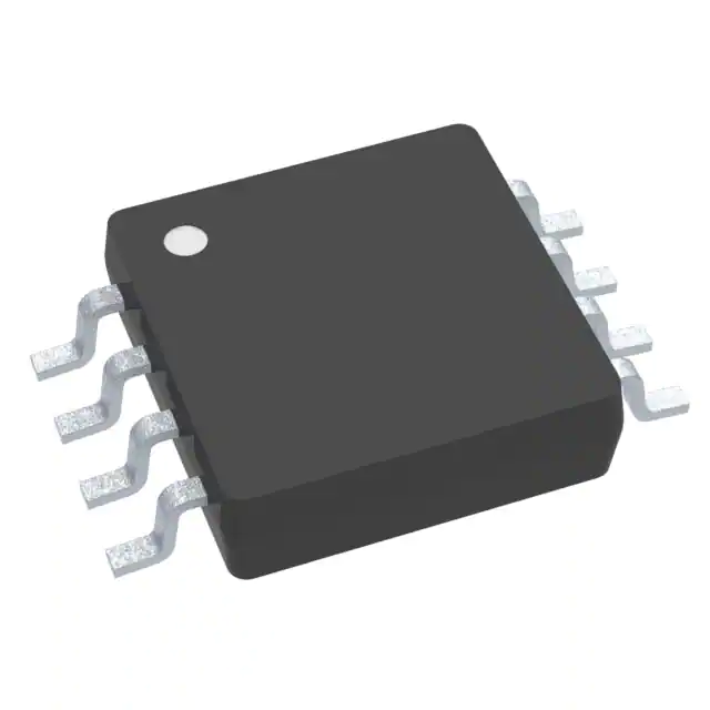
The TCA9517-Q1 is a bidirectional buffer with level shifting capabilities forI2C and SMBus systems. It supplies bidirectional voltage-leveltranslation (up-translation/ down-translation) between low voltages (down to 0.9 V) and highervoltages (2.7 V to 5.25 V) in mixed-mode applications. This device enablesI2C and SMBus systems to be extended without loss of performance, evenduring level shifting.
The TCA9517-Q1 buffers both the serial data (SDA) and the serial clock (SCL) signals onthe I2C bus, thus allowing two buses of up to 400-pF bus capacitance tobe connected in an I2C application.
The TCA9517-Q1 has two types of drivers: A-side drivers and B-side drivers. All inputsand I/Os are overvoltage tolerant to 5.25 V, even when the device is unpowered(VCCB and/or VCCA = 0 V).
The buffer design on the B-side prevents its use in series with devices that use staticvoltage offset. The devices do not recognize buffered low signals as a valid low, and do notpropagate it as a buffered low again.
The B-side drivers operate from 2.7 V to 5.25 V. The output low level for this internalbuffer is approximately 0.5 V. The input voltage must be more than 70 mV below the output low levelwhen the output internally is driven low. The higher-voltage low signal is called a buffered low.When the B-side I/O is driven low internally, the low is not recognized as a low by the input. Thisfeature prevents a lockup condition from occurring when the input low condition is released.
The A-side drivers operate from 0.9 V to 5.25 V, and drive more current. They do notrequire the buffered low feature (or the static offset voltage). A low signal on the B-sidetranslates to a nearly 0 V low on the A-side. This accommodates smaller voltage swings oflower-voltage logic. The output pulldown on the A-side drives a hard low. The input level is set at0.3 × VCCA to accommodate the need for a lower low level in systems wherethe low-voltage-side supply voltage is as low as 0.9 V.
The A-side of two or more TCA9517-Q1 devices can be connected together. This allows manytopographies (See Figure 8 and Figure 9 ) with the A-side as the common bus. TheA-side can be connected directly to any other buffer with static- or dynamic-offset voltage.Multiple TCA9517-Q1 devices can be connected in series, A-side to B-side, with no buildup in offsetvoltage, and with only time-of-flight delays to consider. The TCA9517-Q1 cannot be connected B-sideto B-side, because of the buffered low voltage from the B-side. The B-side cannot be connected to adevice with rise time accelerators.
VCCA is only used to provide the 0.3 × VCCA reference to theA-side input comparators and for the power-good-detect circuit. The TCA9517-Q1 logic and all I/Osare powered by the VCCB pin.
As with the standard I2C system, pullup resistors are requiredto provide the logic-high levels on the buffered bus. The TCA9517-Q1 has standard open-drainconfiguration of the I2C bus. The size of these pullup resistors dependson the system, but each side of the repeater must have a pullup resistor. The device is designed towork with Standard mode and Fast mode I2C devices in addition to SMBusdevices. Standard mode I2C devices only specify 3 mA in a genericI2C system, where Standard mode devices and multiple masters arepossible. Higher termination currents can be used in some cases.
Feature
- AEC-Q100 Qualified for Automotive Applications
- Device Temperature: –40°C to 125°CTA
- Device HBM Classification Level:±5500-V
- Device CDM Classification Level:±1000-V
- Two-Channel BidirectionalBuffer
- I2C Bus and SMBus Compatible
- Operating Supply Voltage Range of 0.9-V to 5.25-V on A-side
- Operating Supply Voltage Range of 2.7-V to5.25-V on B-side
- Voltage-Level Translation From 0.9-V to 5.25-V and2.7-V to 5.25-V
- Active-High Repeater-EnableInput
- Open-Drain I2C I/O
- 5.25-VTolerant I2C and Enable Input Support Mixed-Mode SignalOperation
- Accommodates Standard Mode and Fast ModeI2C Devices and Multiple Masters
- High-ImpedanceI2C Pins When Powered-Off
- Latch-Up PerformanceExceeds 100 mA Per JESD 78, Class II
All trademarks are the property of their respective owners.

