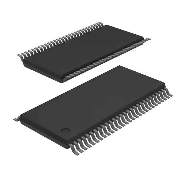
This 18-bit universal bus transceiver is designed for 1.65-V to 3.6-V VCC operation.
Data flow in each direction is controlled by output-enable (OEAB and OEBA\), latch-enable (LEAB and LEBA), and clock (CLKAB\ and CLKBA\) inputs. For A-to-B data flow, the device operates in the transparent mode when LEAB is high. When LEAB is low, the A data is latched if CLKAB\ is held at a high or low logic level. If LEAB is low, the A data is stored in the latch/flip-flop on the high-to-low transition of CLKAB\. Output-enable OEAB is active high. When OEAB is high, the B-port outputs are active. When OEAB is low, the B-port outputs are in the high-impedance state.
Data flow for B to A is similar to that of A to B, but uses OEBA\, LEBA, and CLKBA\. The output enables are complementary (OEAB is active high, and OEBA\ is active low).
To ensure the high-impedance state during power up or power down, OEBA\ should be tied to VCC through a pullup resistor, and OEAB should be tied to GND through a pulldown resistor; the minimum value of the resistor is determined by the current-sinking/current-sourcing capability of the driver.
Active bus-hold circuitry holds unused or floating data inputs at a valid logic state.
The SN74ALVCH16500DLR is characterized for operation from 40°C to 85°C.
Feature
- Member of the Texas Instruments Widebus Family
- EPIC (Enhanced-Performance Implanted CMOS) Submicron Process
- UBT (Universal Bus Transceiver) Transceiver Combines D-Type Latches and D-Type Flip-Flops for Operation in Transparent, Latched, or Clocked Modes
- ESD Protection Exceeds 2000 V Per MIL-STD-883, Method 3015; Exceeds 200 V Using Machine Model (C = 200 pF, R = 0)
- Latch-Up Performance Exceeds 250 mA Per JESD 17
- Bus Hold on Data Inputs Eliminates the Need for External Pullup/Pulldown Resistors
- Package Options Include Plastic 300-mil Shrink Small-Outline (DL) and Thin Shrink Small-Outline (DGG) Packages


