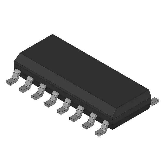
The MAX848/MAX849ESE boost converters set a new standard of high efficiency and high integration for noise-sensitive power-supply applications, such as portable phones and small systems with RF data links. The heart of the these devices is a synchronous boost-topology regulator that generates a fixed 3.3V output (or 2.7V to 5.5V adjustable output) from one to three NiCd/NiMH cells or one Li-Ion cell. Synchronous rectification provides a 5% efficiency improvement over similar nonsynchronous boost regulators. In standby mode, pulse-skipping PFM operation keeps the output voltage alive with only 150μW quiescent power consumption. Fixed-frequency PWM operation ensures that the switching noise spectrum is limited to the 300kHz fundamental and its harmonics, allowing easy post-filtering noise reduction. For even tighter noise spectrum control, synchronize to a 200kHz to 400kHz external clock. Battery monitoring is provided by a two-channel, voltage-to-frequency analog-to-digital converter (ADC). One channel is intended for a single-cell battery input (0.625V to 1.875V range), while the other channel is for monitoring higher voltages (0V to 2.5V range). Two control inputs are provided for push-on, push-off control via a momentary pushbutton switch. Upon power-up, an internal comparator monitors the output voltage to generate a power-good output (POK). The devices differ only in the current limit of the N-channel MOSFET power switch: 0.8A for the MAX848, and 1.4A for the MAX849.
Feature
- Up to 95% Efficiency
- 3.3V Dual Mode? or 2.7V to 5.5V Adj. Output
- 0.7V to 5.5V Input Range
- 0.15mW Standby Mode
- 300kHz PWM Mode or Synchronizable
- Two-Channel ADC with Serial Output
- Power-Good Function
Applications
- Cell Phones
- Digital Cordless Phones
- Handheld Instruments (PDAs, Palmtops)
- Local 3.3V to 5V Supplies
- Palmtop Computers
- PCS Phones
- Personal Communicators


