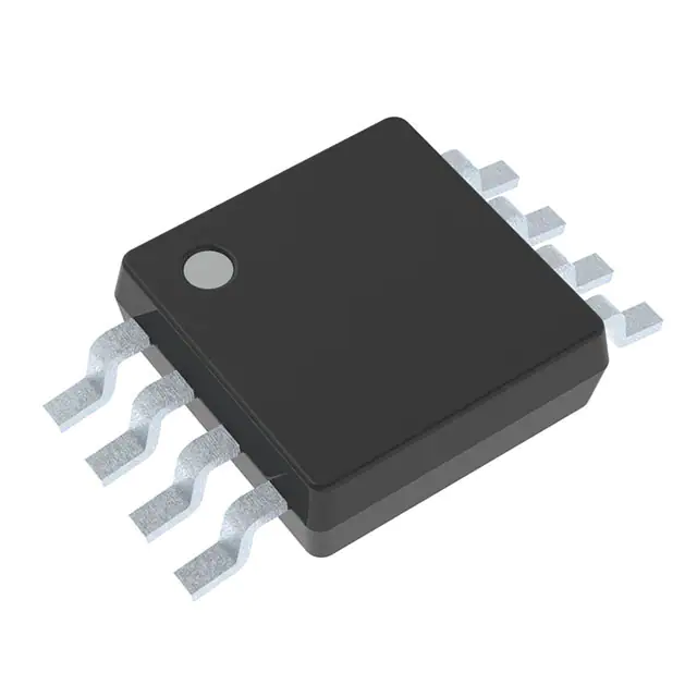
This 2-bit non-inverting bus transceiver uses two separate configurable power-supply rails. The A ports are designed to track VCCA and accepts any supply voltage from 1.2 V to 3.6 V. The B ports are designed to track VCCB and accepts any supply voltage from 1.2 V to 3.6 V. This allows for universal low-voltage bidirectional translation and level-shifting between any of the 1.2 V, 1.5 V, 1.8 V, 2.5 V, and 3.3 V voltage nodes.
The SN74AVCH2T45DCUT is designed for asynchronous communication between two data buses. The logic levels of the direction-control (DIR pin) input activate either the B-port outputs or the A-port outputs. The device transmits data from the A bus to the B bus when the B-port outputs are activated and from the B bus to the A bus when the A-port outputs are activated. The SN74AVCH2T45DCUT features active bus-hold circuitry, which holds unused or un-driven inputs at a valid logic state. TI does not recommend using pull-up or pull-down resistors with the bus-hold circuitry.
This device is fully specified for partial-power-down applications using Ioff. The Ioff circuitry disables the outputs, preventing damaging current backflow through the device when it is powered down. The VCC isolation feature ensures that if either VCC input is at GND, then both outputs are in the high-impedance state. The bus-hold circuitry on the powered-up side always stays active.
Active bus-hold circuitry holds unused or un-driven inputs at a valid logic state. NanoFree package technology is a major breakthrough in IC packaging concepts, using the die as the package.
Feature
- Available in the Texas Instruments NanoFree Package
- VCC Isolation
- 2-Rail Design
- I/Os are 4.6 V Tolerant
- Partial Power-Down-Mode Operation
- Bus Hold on Data Inputs
- Maximum Data Rates
- 500 Mbps (1.8 V to 3.3 V)
- 320 Mbps (< 1.8 V to 3.3 V)
- 320 Mbps (Level-Shifting to 2.5 V or 1.8 V)
- 280 Mbps (Level-Shifting to 1.5 V)
- 240 Mbps (Level-Shifting to 1.2 V)
- Latch-Up Performance Exceeds 100 mA Per JESD 78, Class II
- ESD Protection Exceeds JESD 22
This 2-bit non-inverting bus transceiver uses two separate configurable power-supply rails. The A ports are designed to track VCCA and accepts any supply voltage from 1.2 V to 3.6 V. The B ports are designed to track VCCB and accepts any supply voltage from 1.2 V to 3.6 V. This allows for universal low-voltage bidirectional translation and level-shifting between any of the 1.2 V, 1.5 V, 1.8 V, 2.5 V, and 3.3 V voltage nodes.
The SN74AVCH2T45 is designed for asynchronous communication between two data buses. The logic levels of the direction-control (DIR pin) input activate either the B-port outputs or the A-port outputs. The device transmits data from the A bus to the B bus when the B-port outputs are activated and from the B bus to the A bus when the A-port outputs are activated. The SN74AVCH2T45 features active bus-hold circuitry, which holds unused or un-driven inputs at a valid logic state. TI does not recommend using pull-up or pull-down resistors with the bus-hold circuitry.
This device is fully specified for partial-power-down applications using Ioff. The Ioff circuitry disables the outputs, preventing damaging current backflow through the device when it is powered down. The VCC isolation feature ensures that if either VCC input is at GND, then both outputs are in the high-impedance state. The bus-hold circuitry on the powered-up side always stays active.
Active bus-hold circuitry holds unused or un-driven inputs at a valid logic state. NanoFree package technology is a major breakthrough in IC packaging concepts, using the die as the package.


