Widebus, EPIC-IIB, and UBT are trademarks of Texas Instruments Incorporated.
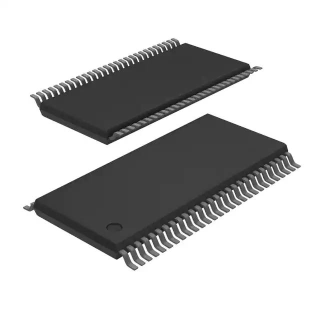
Texas InstrumentsSN74ABT16601DLThese 18-bit universal bus transceivers combine D-type latches and D-type flip-flops to allow data flow in transparent, latched, clocked, and clock-enabled modes.
Data flow in each direction is controlled by output-enable ( and ), latch-enable (LEAB and LEBA), and clock (CLKAB and CLKBA) inputs. The clock can be controlled by the clock-enable ( and ) inputs. For A-to-B data flow, the device operates in the transparent mode when LEAB is high. When LEAB is low, the A data is latched if CLKAB is held at a high or low logic level. If LEAB is low, the A data is stored in the latch/flip-flop on the low-to-high transition of CLKAB. Output enableis active low. Whenis low, the outputs are active. Whenis high, the outputs are in the high-impedance state.
Data flow for B to A is similar to that of A to B, but uses , LEBA, CLKBA, and .
To ensure the high-impedance state during power up or power down,should be tied to VCC through a pullup resistor; the minimum value of the resistor is determined by the current-sinking capability of the driver.
The SN54ABT16601 is characterized for operation over the full military temperature range of -55°C to 125°C. The SN74ABT16601DL is characterized for operation from -40°C to 85°C.
Feature
- Members of the Texas Instruments WidebusTM Family
- State-of-the-Art EPIC-IIBTM BiCMOS DesignSignificantly Reduces Power Dissipation
- UBTTM (Universal Bus Transceiver) Combines D-TypeLatches and D-Type Flip-Flops for Operation in Transparent,Latched, Clocked, or Clock-Enabled Mode
- Latch-Up Performance Exceeds 500 mA Per JEDEC Standard JESD-17
- Typical VOLP (Output Ground Bounce) < 0.8 V atVCC = 5 V, TA = 25°C
- Flow-Through Architecture Optimizes PCB Layout
- Package Options Include Plastic 300-mil Shrink Small-Outline(DL) and Thin Shrink Small-Outline (DGG) Packages and 380-milFine-Pitch Ceramic Flat (WD) Package Using 25-mil Center-to-CenterSpacings


