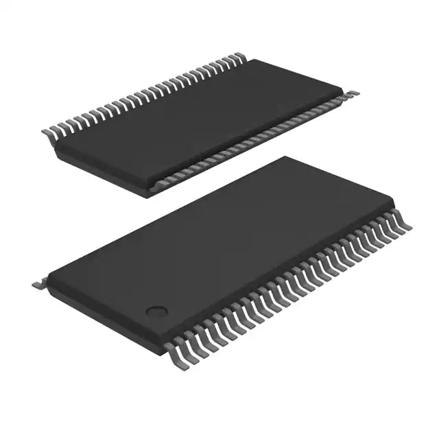
The 'LVT16501 are 18-bit universal bus transceivers designed for low-voltage (3.3-V) VCC operation, but with the capability to provide a TTL interface to a 5-V system environment.
Data flow in each direction is controlled by output-enable (OEAB and ), latch-enable (LEAB and LEBA), and clock (CLKAB and CLKBA) inputs. For A-to-B data flow, the devices operate in the transparent mode when LEAB is high. When LEAB is low, the A data is latched if CLKAB is held at a high or low logic level. If LEAB is low, the A-bus data is stored in the latch/flip-flop on the low-to-high transition of CLKAB. When OEAB is high, the outputs are active. When OEAB is low, the outputs are in the high-impedance state.
Data flow for B to A is similar to that of A to B but uses , LEBA, and CLKBA. The output enables are complementary (OEAB is active high andis active low).
Active bus-hold circuitry is provided to hold unused or floating data inputs at a valid logic level.
To ensure the high-impedance state during power up or power down,should be tied to VCC through a pullup resistor. The minimum value of the resistor is determined by the current-sinking capability of the driver. OE should be tied to GND through a pulldown resistor; the minimum value of the resistor is determined by the current-sourcing capability of the driver.
The SN74LVT16501DLR is available in TI's shrink small-outline (DL) and thin shrink small-outline (DGG) packages, which provide twice the input/output (I/O) pin count and functionality of standard small-outline packages in the same printed circuit board area.
The SN54LVT16501 is characterized for operation over the full military temperature range of -55°C to 125°C. The SN74LVT16501DLR is characterized for operation from -40°C to 85°C.
Feature
- State-of-the-Art Advanced BiCMOS Technology (ABT) Design for3.3-V Operation and Low-Static Power Dissipation
- Members of the Texas Instruments WidebusTM Family
- Support Mixed-Mode Signal Operation (5-V Input and OutputVoltages With 3.3-V VCC)
- Support Unregulated Battery Operation Down to 2.7 V
- UBTTM (Universal Bus Transceiver) Combines D-TypeLatches and D-Type Flip-Flops for Operation in Transparent,Latched, or Clocked Mode
- Typical VOLP (Output Ground Bounce) < 0.8 V atVCC = 3.3 V, TA = 25°C
- ESD Protection Exceeds 2000 V Per MIL-STD-883, Method 3015;Exceeds 200 V Using Machine Model (C = 200 pF, R = 0)
- Latch-Up Performance Exceeds 500 mA Per JEDEC Standard JESD-17
- Bus Hold on Data Inputs Eliminates the Need for ExternalPullup/Pulldown Resistors
- Support Live Insertion
- Distributed VCC and GND Pin Configuration MinimizesHigh-Speed Switching Noise
- Flow-Through Architecture Optimizes PCB Layout
- Package Options Include Plastic 300-mil Shrink Small-Outline(DL) and Thin Shrink Small-Outline (DGG) Packages and 380-milFine-Pitch Ceramic Flat (WD) Package Using 25-mil Center-to-CenterSpacings


