All trademarks are the property of their respective owners.
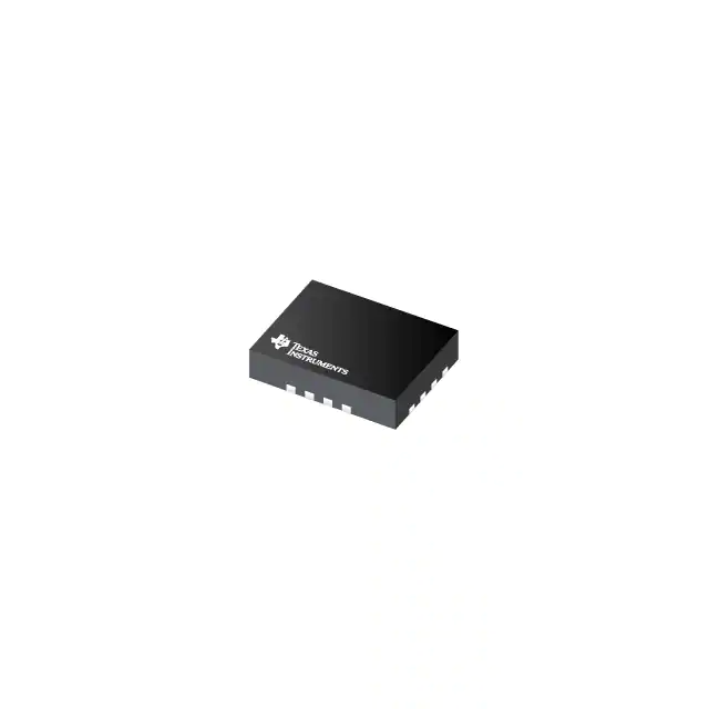
DescriptionThis 4-bit noninverting bus transceiver uses two separate configurable power-supplyrails. The A port is designed to track VCCA. VCCAaccepts any supply voltage from 1.2 V to 3.6 V. The B port is designed to trackVCCB. VCCB accepts any supply voltage from 1.2 to 3.6V. The SN74AVC4T774RSVR is optimized to operate withVCCA/VCCB set at 1.4 V to 3.6 V. It is operationalwith VCCA/VCCB as low as 1.2 V. This allows foruniversal low-voltage bi-directional translation between any of the 1.2-V, 1.5-V, 1.8-V, 2.5-V, and3.3-V voltage nodes.
The SN74AVC4T774RSVR is designed for asynchronous communication between data buses. The logiclevels of the direction-control (DIR) input and the output-enable (OE should be tied to VCCA through a pullup resistor;the minimum value of the resistor is determined by the current-sinking capability of the driver.Since this device has CMOS inputs, it is very important to not allow them to float. If the inputsare not driven to either a high VCC state, or a low-GND state, anundesirable larger than expected ICC current may result. Since the inputvoltage settlement is governed by many factors (for example, capacitance, board-layout, packageinductance, surrounding conditions, and so forth), ensuring that they these inputs are kept out oferroneous switching states and tying them to either a high or a low level minimizes theleakage-current.
Feature
- Each Channel Has an Independent DIR Control Input
- Control Inputs VIH/VIL Levels areReferenced to VCCA Voltage
- Fully Configurable Dual-Rail Design Allows Each Port to Operate Over the Full 1.2-Vto 3.6-V Power-Supply Range
- I/Os are 4.6-V Tolerant
- Ioff Supports Partial Power-Down-Mode Operation
- Typical Data Rates
- 380 Mbps (1.8-V to 3.3-V Translation)
- 200 Mbps (<1.8-V to 3.3-VTranslation)
- 200 Mbps (Translate to 2.5 V or 1.8V)
- 150 Mbps (Translate to 1.5 V)
- 100 Mbps (Translate to 1.2V)
- Latch-Up Performance Exceeds 100 mA Per JESD 78, Class II
- ESD Protection Exceeds the Following Levels (Tested Per JESD22)
- ±8000-V Human-Body Model (A114-A)
- 250-V MachineModel (A115-A)
- ±1500-V Charged-Device Model(C101)
All trademarks are the property of their respective owners.
DescriptionThis 4-bit noninverting bus transceiver uses two separate configurable power-supplyrails. The A port is designed to track VCCA. VCCAaccepts any supply voltage from 1.2 V to 3.6 V. The B port is designed to trackVCCB. VCCB accepts any supply voltage from 1.2 to 3.6V. The SN74AVC4T774 is optimized to operate withVCCA/VCCB set at 1.4 V to 3.6 V. It is operationalwith VCCA/VCCB as low as 1.2 V. This allows foruniversal low-voltage bi-directional translation between any of the 1.2-V, 1.5-V, 1.8-V, 2.5-V, and3.3-V voltage nodes.
The SN74AVC4T774 is designed for asynchronous communication between data buses. The logiclevels of the direction-control (DIR) input and the output-enable (OE should be tied to VCCA through a pullup resistor;the minimum value of the resistor is determined by the current-sinking capability of the driver.Since this device has CMOS inputs, it is very important to not allow them to float. If the inputsare not driven to either a high VCC state, or a low-GND state, anundesirable larger than expected ICC current may result. Since the inputvoltage settlement is governed by many factors (for example, capacitance, board-layout, packageinductance, surrounding conditions, and so forth), ensuring that they these inputs are kept out oferroneous switching states and tying them to either a high or a low level minimizes theleakage-current.


