The Gunning Transceiver Logic - Transceiver Voltage Clamps (GTL-TVC) providehigh-speed voltage translation with low ON-state resistance and minimal propagationdelay. The GTL2003BQ,115 provides eight NMOS pass transistors (Sn and Dn) with a commongate (GREF) and a reference transistor (SREF and DREF). The device allowsbidirectional voltage translations between 0.8 V and 5.0 V without use of a direction pin.Voltage translation below 0.8 V can be achieved when properly biased. For moreinformation, refer to application note AN11127.
When the Sn or Dn port is LOW, the clamp is in the ON-state and a low resistanceconnection exists between the Sn and Dn ports. Assuming the higher voltage is on the Dnport, when the Dn port is HIGH, the voltage on the Sn port is limited to the voltage set bythe reference transistor (SREF). When the Sn port is HIGH, the Dn port is pulled to VDD1by the pull-up resistors. This functionality allows a seamless translation between higherand lower voltages selected by the user, without the need for directional control.
All transistors have the same electrical characteristics and there is minimal deviation fromone output to another in voltage or propagation delay. This is a benefit over discretetransistor voltage translation solutions, since the fabrication of the transistors issymmetrical. Because all transistors in the device are identical, SREF and DREF can belocated on any of the other eight matched Sn/Dn transistors, allowing for easier boardlayout. The translator's transistors provide excellent ESD protection to lower voltagedevices and at the same time protect less ESD-resistant devices.
Feature
- 8-bit bidirectional low voltage translator
- Allows voltage level translation between 0.8 V, 0.9 V, 1.0 V, 1.2 V, 1.5 V, 1.8 V, 2.5 V,3.3 V, and 5 V buses which allows direct interface with GTL, GTL+, LVTTL/TTL and5 V CMOS levels
- Provides bidirectional voltage translation with no direction pin
- Low 6.5 Ω ON-state resistance (Ron) between input and output pins (Sn/Dn)
- Supports hot insertion
- No power supply required: will not latch up
- 5 V tolerant inputs
- Low standby current
- Flow-through pinout for ease of printed-circuit board trace routing
- ESD protection exceeds 2000 V HBM per JESD22-A114, and 1000 V CDM perJESD22-C101
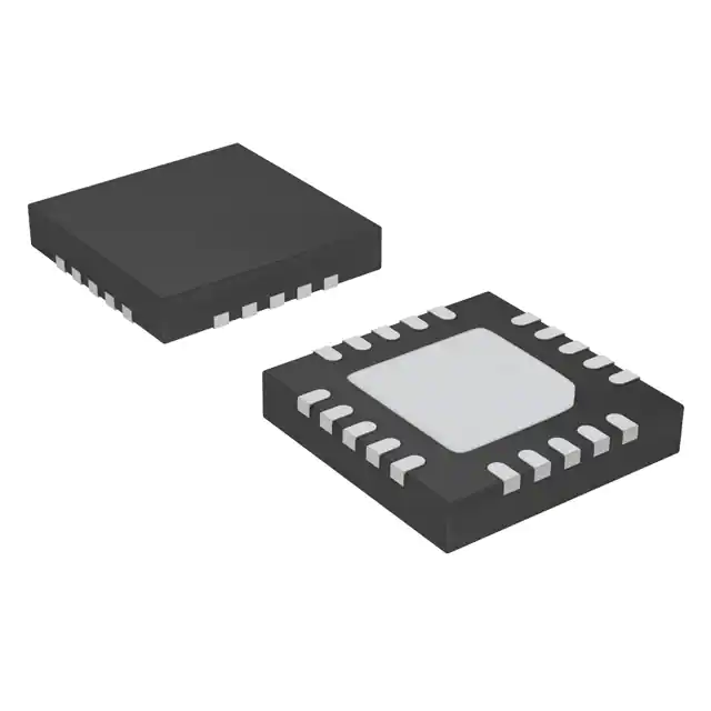
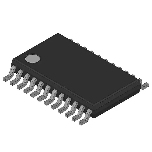
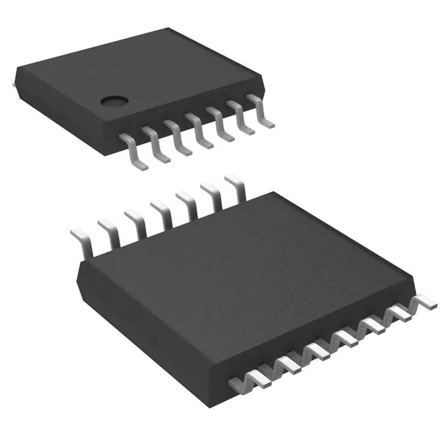
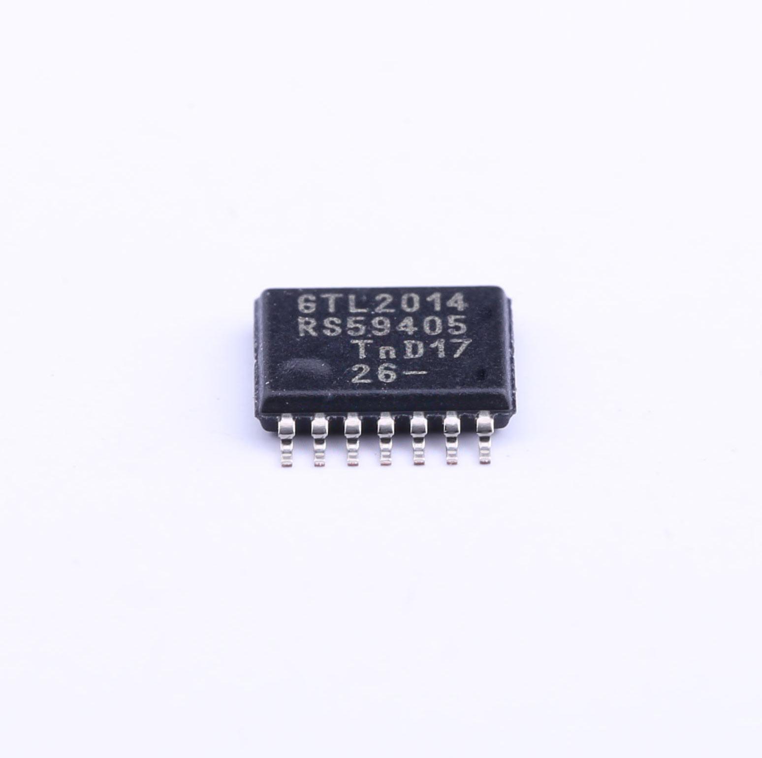
- Packages offered: TSSOP20, DHVQFN20
- Any application that requires bidirectional or unidirectional voltage level translationfrom any voltage from 0.8 V to 5.0 V to any voltage from 0.8 V to 5.0 V
- The open-drain construction with no direction pin is ideal for bidirectional low voltage(for example, 0.8 V, 0.9 V, 1.0 V, 1.2 V, 1.5 V, or 1.8 V) processor I²C-bus porttranslation to the normal 3.3 V and/or 5.0 V I²C-bus signal levels or GTL/GTL+translation to LVTTL/TTL signal levels.


