All trademarks are the property of their respective owners.
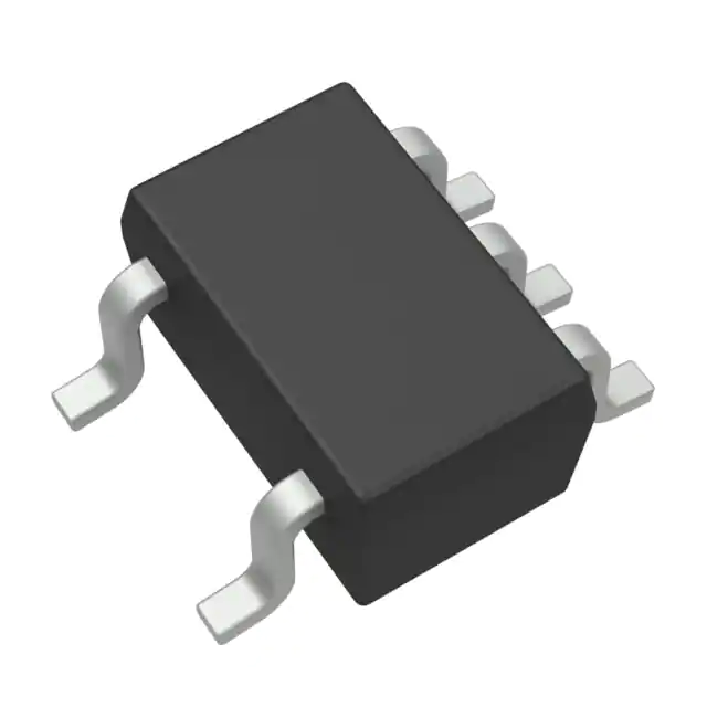
DescriptionThe SN74AUP1T34DCKR device is a 1-bitnoninverting translator that uses two separate configurable power-supply rails. It is auni-directional translator from A to B. The A port is designed to trackVCCA. VCCA accepts supply voltages from 0.9 V to 3.6V. The B port is designed to track VCCB. VCCB acceptssupply voltages from 0.9 V to 3.6 V. This allows for low-voltage translation between 1-V, 1.2-V,1.5-V, 1.8-V, 2.5-V, and 3.3-V voltage nodes. The SN74AUP1T34DCKR is also fully specified forpartial-power-down applications using Ioff. The Ioffcircuitry disables the outputs, preventing damaging current backflow through the device when it ispowered down.
The VCC isolation feature ensures that if VCCA input is at GND,the B port is in the high-impedance state. If VCCB input is at GND, anyinput to the A side does not cause the leakage current even floating.
Feature
- Wide Operating VCC Range of 0.9 V to 3.6 V
- Balanced Propagation Delays: tPLH =tPHL (1.8-V to 3.3-V Translation Typical)
- LowStatic-Power Consumption: Maximum of 5-μA ICC
- ±6-mA Output Drive at 3V
- Ioff Supports Partial Power-Down-ModeOperation
- VCC Isolation Feature – If VCCA Input Is atGND, B Port Is in the High-Impedance state
- Input Hysteresis Allows Slow Input Transition and BetterSwitching Noise Immunity at Input
- ESD Protection Exceeds JESD22
- 5000-V Human-Body Model (A114-A)
- Latch-Up PerformanceExceeds 100 mA Per JESD 78, Class II
All trademarks are the property of their respective owners.
DescriptionThe SN74AUP1T34 device is a 1-bitnoninverting translator that uses two separate configurable power-supply rails. It is auni-directional translator from A to B. The A port is designed to trackVCCA. VCCA accepts supply voltages from 0.9 V to 3.6V. The B port is designed to track VCCB. VCCB acceptssupply voltages from 0.9 V to 3.6 V. This allows for low-voltage translation between 1-V, 1.2-V,1.5-V, 1.8-V, 2.5-V, and 3.3-V voltage nodes. The SN74AUP1T34 is also fully specified forpartial-power-down applications using Ioff. The Ioffcircuitry disables the outputs, preventing damaging current backflow through the device when it ispowered down.
The VCC isolation feature ensures that if VCCA input is at GND,the B port is in the high-impedance state. If VCCB input is at GND, anyinput to the A side does not cause the leakage current even floating.


