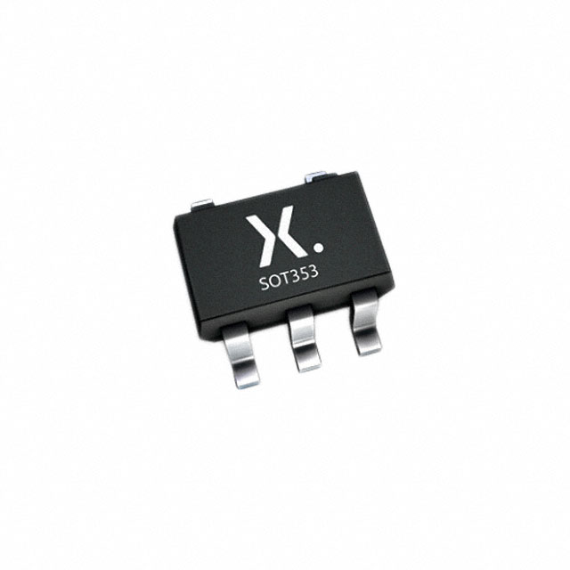
The 74AUP1T34GW is a low-power single Translating Buffer with two separate supply voltages. Input A is designed to track VCC(A). Output Y is designed to track VCC(Y). Both VCC(A) and VCC(Y) accepts any supply voltage from 1.1 to 3.6V. This feature allows universal low voltage interfacing between any of the 1.2/1.5/1.8/2.5/3.3V voltage nodes. Schmitt trigger action at all inputs makes the circuit tolerant to slower input rise and fall times across the entire VCC range from 1.1 to 3.6V. This device ensures very low static and dynamic power consumption across the entire VCC range from 1.1 to 3.6V. This device is fully specified for partial power-down applications using IOFF. The IOFF circuitry disables the output, preventing the damaging backflow current through the device when it is powered down.
Feature
- High noise immunity
- IOFF circuitry provides partial power-down mode operation
- Complies with JEDEC standards
- Low static power consumption, ICC = 0.9µA maximum
- Latch-up performance exceeds 100mA per JESD 78 class II
- Inputs accept voltages up to 3.6V
- Low noise overshoot and undershoot <10% of VCC
Applications
Industrial, Automation & Process Control, Signal Processing


