Product Description
The Serial Quad I/O™ (SQI™) family of flash-memory devices features a six-wire, 4-bit I/O interface that allows for low-power, high-performance operation in a low pin-count package. SST26VF032B/032BA also support full command-set compatibility to traditional Serial Peripheral Interface (SPI) protocol. System designs using SQI flash devices occupy less board space and ultimately lower system costs.
All members of the 26 Series, SQI family are manufactured with proprietary, high-performance CMOS SuperFlash® technology. The split-gate cell design and thick-oxide tunneling injector attain better reliability and manufacturability compared with alternate approaches.
SST26VF032B/032BA significantly improve performance and reliability, while lowering power consumption. These devices write (Program or Erase) with a single power supply of 2.3-3.6V. The total energy consumed is a function of the applied voltage, current, and time of application. Since for any given voltage range, the SuperFlash technology uses less current to program and has a shorter erase time, the total energy consumed during any Erase or Program operation is less than alternative flash memory technologies.
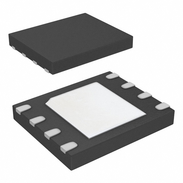
SST26VF032B/032BA are offered in 8-contact WDFN (6 mm x 5 mm), 8-lead SOIJ (5.28 mm), and 24-ball TBGA(6mm x 8mm). See Figure 2-2 for pin assignments.
Two configurations are available upon order. SST26VF032B-104I/MF default at power-up has the WP# and HOLD# pins enabled, and the SIO2 and SIO3 pins disabled, to initiate SPI-protocol operations. SST26VF032BA default at power-up has the WP# and HOLD# pins disabled, and the SIO2 and SIO3 pins enabled, to initiate Quad I/O operations. See “I/O Configuration (IOC)” on page 13 for more information about configuring WP#/HOLD# and SIO2/SIO3 pins.
Features
• Single Voltage Read and Write Operations
- 2.7-3.6V or 2.3-3.6V
• Serial Interface Architecture
- Nibble-wide multiplexed I/O’s with SPI-like serial command structure
- Mode 0 and Mode 3
- x1/x2/x4 Serial Peripheral Interface (SPI) Protocol
• High Speed Clock Frequency
- 2.7-3.6V: 104 MHz max
- 2.3-3.6V: 80 MHz max
• Burst Modes
- Continuous linear burst
- 8/16/32/64 Byte linear burst with wrap-around
• Superior Reliability
- Endurance: 100,000 Cycles (min)
- Greater than 100 years Data Retention
• Low Power Consumption:
- Active Read current: 15 mA (typical @ 104 MHz)
- Standby Current: 15 µA (typical)
• Fast Erase Time
- Sector/Block Erase: 18 ms (typ), 25 ms (max)
- Chip Erase: 35 ms (typ), 50 ms (max)
• Page-Program
- 256 Bytes per page in x1 or x4 mode
• End-of-Write Detection
- Software polling the BUSY bit in status register
• Flexible Erase Capability
- Uniform 4 KByte sectors
- Four 8 KByte top and bottom parameter overlay blocks
- One 32 KByte top and bottom overlay block
- Uniform 64 KByte overlay blocks
• Write-Suspend
- Suspend Program or Erase operation to access another block/sector
• Software Reset (RST) mode
• Software Write Protection
- Individual-Block Write Protection with permanent lock-down capability
- 64 KByte blocks, two 32 KByte blocks, and eight 8 KByte parameter blocks
- Read Protection on top and bottom 8 KByte parameter blocks
• Security ID
- One-Time Programmable (OTP) 2 KByte, Secure ID
- 64 bit unique, factory pre-programmed identifier
- User-programmable area
• Temperature Range
- Industrial: -40°C to +85°C
- Industrial Plus: -40°C to +105°C
• Automotive AECQ-100 Grade 2 and Grade 3
• Packages Available
- 8-contact WDFN (6mm x 5mm)
- 8-lead SOIJ (5.28 mm)
- 24-ball TBGA (6mm x 8mm)
• All devices are RoHS compliant
Feature
- Serial interface architecture - mode 0/3
- Nibble-wide multiplexed I/O with SPI-like serial command structure
- High speed clock frequency - 104MHz maximum
- Burst modes - continuous linear burst
- Superior reliability
- Endurance - 100000 cycles minimum
- Greater than 100 years data retention
- Low power consumption
- Fast erase time
- End-of-write detection - software polling the BUSY bit in status register
- Flexible erase capability
- Write-suspend - suspend program or erase operation to access another block/sector
- Software reset (RST) mode
- Software write protection
- Individual-block write protection with permanent lock-down capability
- Read protection on top and bottom 8-Kbyte parameter blocks
- Security ID
- User-programmable area
Applications
(Picture:Pinout / Diagram)

